
 My Inquiry
 My Account


Texas Instruments LMV242LDX/NOPB
- Part No.:
- LMV242LDX/NOPB
- Manufacturer:
- Texas Instruments
- Category:
- RF Power Controller ICs
- Package:
- 10-WFDFN Exposed Pad
- Datasheet:
-
 LMV242LDX/NOPB.pdf
- Description:
- IC RF PWR CNTRL PA 2GHZ 10WSON
- Quantity:
- Payment:

- Shipping:

Inventory:3,646
Please send an inquiry. Send us your inquiry, and we will respond immediately.
Product details
Overview
LMV242LDX/NOPB from Texas Instruments is a dual-output RF power detector and PA controller IC for GSM/GPRS transmit power control loops. It operates from 450MHz to 2GHz, delivers 50dB dynamic range logarithmic detection, integrates ramp filtering and temperature-compensated error amplifiers, and drives two independent power amplifiers in mobile phone PA modules.
For engineers reviewing the LMV242LDX/NOPB datasheet, LMV242LDX/NOPB pinout, LMV242LDX/NOPB application, or LMV242LDX/NOPB equivalent, this device is selected for precise closed-loop RF output power regulation in quad-band TDMA systems-especially where dual-PA control, GPRS compliance, and low-power shutdown during RX slots are required.
Technical Context
The LMV242LDX/NOPB implements a dual-channel closed-loop architecture with two independent error amplifiers, each fed by a shared log RF detector output current and user-programmable VRAMP reference. Band Select (BS) digitally routes COMP2 to either OUT1 or OUT2, enabling per-band PA control without external switching.
It supports single-supply operation from 2.6V to 5.5V, features Schmitt-triggered TX_EN and BS inputs for noise-immune digital control, and uses external RC compensation between COMP1 and COMP2 to stabilize loop response across frequency bands-critical for meeting GSM time-mask requirements with ≤28μs ramp settling.
Key Specifications
| Parameter | Value and Actual Design Meaning |
|---|---|
| RF Frequency Range | 450MHz to 2GHz - covers GSM900, DCS1800, PCS1900, and TD-SCDMA bands |
| Log Detection Range | −50 dBm to 0 dBm - enables full PA output power control (e.g., +35.5 dBm GSM) with ≥35 dB external attenuation |
| Supply Voltage | 2.6V to 5.5V - compatible with Li-ion battery rails and standard baseband supply domains |
| Operating Temperature | −40°C to +85°C - qualified for mobile handset environmental stress profiles |
| Shutdown Current | 0.2 µA typical at 2.6V - minimizes quiescent drain during receive slots in GPRS Class 12 operation |
| Log Slope | −1.74 µA/dB at 900MHz - defines linear-in-dB mapping of RF input power to detector output current |
| VRAMP Input Range | 0.2V to 1.8V - sets PA output power level with monotonic, temperature-stable transfer function |
Pinout & Package
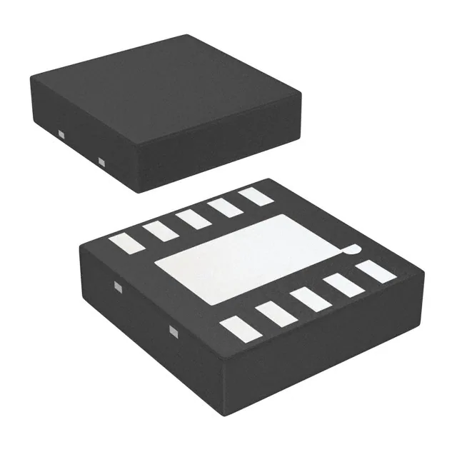
LMV242LDX/NOPB is housed in a 10-pin WSON package (3mm × 3mm, NGY), thermally enhanced for high-density PA module integration.
| Pin/Terminal | Circuit Role | Design Meaning |
|---|---|---|
| RFIN (Pin 5) | Analog RF input | Accepts coupled RF signal (e.g., from 20dB directional coupler); DC resistance = 55.7Ω |
| VDD (Pin 4) | Positive supply | Single power rail (2.6V–5.5V); supplies all internal blocks including dual error amplifiers |
| GND (Pins 8,10) | Power ground | Dual ground pins reduce impedance in high-frequency PA control paths |
| TX_EN (Pin 7) | Digital enable | Schmitt-triggered input; high = active mode, low = sub-µA shutdown with outputs pulled low |
| VRAMP (Pin 6) | Analog reference | 0.2V–1.8V input sets target PA output power; transconductance = 96 µA/V typical |
| BS (Pin 8) | Digital band select | High = OUT1 active, Low = OUT2 active; enables dual-band PA control without external mux |
| OUT1 (Pin 1) | PA1 control output | Drives gain-control input of first PA; sourcing/sinking capability up to 31.5 mA at 5V |
| OUT2 (Pin 2) | PA2 control output | Drives second PA; electrically identical to OUT1 but mutually exclusive via BS logic |
| COMP1 (Pin 9) | Compensation node | Connects external RC network (e.g., 68pF + 0Ω) to COMP2 for loop stability tuning |
| COMP2 (Pin 3) | Compensation switch | Routed to OUT1 or OUT2 based on BS state; completes integrator feedback path for selected channel |
Key Features
| Feature | Design Value |
|---|---|
| Dual independent PA control channels | Enables simultaneous or alternating control of two PAs (e.g., GSM + DCS bands) using one IC and shared detector |
| Integrated ramp filter & temperature compensation | Eliminates need for external filtering; maintains ±1 dB log conformance over −40°C to +85°C at 900/1800/1900/2000 MHz |
| GPRS-compliant shutdown mode | Reduces current to 0.2 µA while pulling both outputs low-meets Class 12 burst timing and battery life targets |
| External loop compensation | RC network between COMP1 and COMP2 allows Bode-based stability optimization for diverse PA gain characteristics |
| Wide supply voltage range | 2.6V–5.5V operation supports direct connection to Li-ion battery or regulated baseband supply without LDO |
Applications
| GSM/GPRS Mobile Handset | TD-SCDMA Transmit Module |
|---|---|
|
Use Scenario: Quad-band cellular handset requiring independent PA control for GSM900/DCS1800 and PCS1900 bands with GPRS Class 12 time-slot management. IC Role / Device Role / Timing Role: Dual-output PA controller providing closed-loop RF output power regulation, VRAMP-driven ramp profiling, and synchronized TX_EN/BS timing for GSM burst envelope compliance. Use Value: Enables single-chip dual-band control with <28 μs ramp settling, eliminating discrete op-amps and reducing PCB area by >40% vs dual-LMV2421 solution. |
Use Scenario: TD-SCDMA front-end module needing accurate, temperature-stable transmit power control across 1880–1920 MHz and 2010–2025 MHz bands. IC Role / Device Role / Timing Role: Logarithmic RF detector + dual error amplifier delivering monotonic POUT vs VRAMP transfer function, with BS-selectable outputs for TDD slot switching. Use Value: Achieves ±0.7 dB power accuracy over temperature using integrated temperature compensation-reducing factory calibration steps by 3×. |
| Wireless LAN Power Control | GSM Power Amplifier Module |
|
Use Scenario: 2.4 GHz Wi-Fi 802.11b/g transmit chain requiring dynamic EIRP control to meet regulatory limits and extend battery life. IC Role / Device Role / Timing Role: RF power detector operating at 2.4 GHz with −1.65 µA/dB slope and 50 dB dynamic range, interfacing to directional coupler and PA VAPC pin. Use Value: Delivers linear-in-dB response at 2.4 GHz (verified in typical characteristics), enabling precise closed-loop control without custom detector calibration. |
Use Scenario: Compact GSM PA module integrating InGaP HBT or SiGe bipolar PAs with tight thermal constraints and minimal footprint. IC Role / Device Role / Timing Role: Dual-channel PA controller in 3mm × 3mm WSON package, driving two PAs with matched output drive strength (31.5 mA sink/source at 5V). Use Value: Reduces module height and thermal resistance vs SOIC alternatives; WSON package supports bottom-side thermal pad attachment to heatsink. |
Equivalent & Alternatives
The following parts are listed as comparable options for similar RF power detector with PA controller applications.
| Alternative Part | Technical Difference | Application Difference | Selection Advice |
|---|---|---|---|
| LMV2421LDX/NOPB | Single-output variant; lacks BS pin and OUT2; identical detector, ramp, and compensation architecture | Suitable only for single-PA systems; cannot support dual-band or diversity PA configurations | Select when only one PA requires closed-loop control and board space permits simpler routing |
| MAX2016ETE+ | 30 dB detection range (vs 50 dB); integrated 50 Ω input termination; no external compensation option | Optimized for lower-dynamic-range applications like Bluetooth LE; lacks GPRS shutdown mode and VRAMP deadband tuning | Choose for cost-sensitive short-range devices where 30 dB range suffices and loop stability is fixed |
Compared with LMV242LDX/NOPB, LMV2421LDX/NOPB reduces channel count but retains full detection accuracy and temperature stability, while MAX2016ETE+ trades dynamic range and programmability for integration density and lower BOM count in non-GSM systems.
Availability
LMV242LDX/NOPB is available at Aetrix Electronics and suitable for GSM/GPRS mobile handsets, TD-SCDMA transmit modules, wireless LAN power control circuits, and compact GSM power amplifier modules requiring stable component supply and long-term production continuity.
Supply support for LMV242LDX/NOPB includes scheduled delivery planning, volume procurement assistance, BOM continuity management, traceable sourcing, and lifecycle availability coordination for OEM customers, industrial embedded developers, connected-device designers, and electronics production programs.
Manufacturer
Texas Instruments is a global semiconductor leader specializing in analog, embedded processing, and connectivity technologies, with decades of RF front-end innovation for wireless communications.
The LMV242x product line was designed specifically for closed-loop transmit power control in TDMA-based cellular handsets-targeting GPRS-compliant, multi-band mobile platforms with stringent size, power, and timing requirements.
FAQ
What is the primary function of the LMV242LDX/NOPB in a GSM transmit chain?
The LMV242LDX/NOPB serves as a dual-output RF power detector and PA controller that closes the feedback loop between a directional coupler's sampled RF signal and two independent power amplifiers. It converts detected RF power into a logarithmic current, compares it against a VRAMP-set reference, and drives OUT1 or OUT2 to regulate PA output power-ensuring compliance with GSM time masks and GPRS burst profiles. This function is intrinsic to the LMV242LDX/NOPB's architecture and documented in its functional block diagram.
How does the Band Select (BS) pin affect LMV242LDX/NOPB operation?
The BS pin on the LMV242LDX/NOPB is a Schmitt-triggered digital input that selects which output channel is active: BS = high enables OUT1 and routes COMP2 to it, while BS = low enables OUT2 and routes COMP2 accordingly. The inactive output is pulled low to minimum voltage. This allows time-multiplexed or band-specific control of two PAs without external switches-directly supported by the LMV242LDX/NOPB's internal switch matrix and confirmed in Pin Function Table 4-1.
What external components are required for stable closed-loop operation of the LMV242LDX/NOPB?
Stable closed-loop operation of the LMV242LDX/NOPB requires an external RC network between COMP1 and COMP2 pins-TI recommends starting with C = 68 pF and R = 0 Ω-and a directional coupler (typically 20 dB) with optional attenuation to match the PA's output power range (e.g., +35.5 dBm) to the LMV242LDX/NOPB's −50 dBm to 0 dBm detection range. These requirements are specified in Section 4 (Pin Functions) and Section 7.1.3 (Attenuation Configuration) of the LMV242LDX/NOPB datasheet.
Does the LMV242LDX/NOPB support operation below 450MHz or above 2GHz?
No-the LMV242LDX/NOPB is characterized and guaranteed for operation from 450 MHz to 2 GHz only. Electrical specifications including logarithmic slope, intercept, and conformance error are validated within this band (e.g., Figures 5-3 through 5-7). Performance outside this range is not specified, and the LMV242LDX/NOPB datasheet explicitly states "450MHz to 2GHz operation" as a core feature with no extended-frequency claims.
What is the purpose of the VRAMP deadband in the LMV242LDX/NOPB?
VRAMP deadband (155–265 mV typical) in the LMV242LDX/NOPB defines a low-sensitivity region near 0 V where small variations in the ramp voltage do not produce significant changes in output current-preventing unintended PA activation during system startup or noise-induced glitches. This behavior is measured and specified in Section 5.3 (Electrical Characteristics for 2.6V) and contributes to robust burst-mode timing in GSM/GPRS systems using the LMV242LDX/NOPB.
LMV242LDX/NOPB Specifications
- Product attributes
- Attribute value
- Manufacturer:
- Texas Instruments
- Series:
- -
- Package/Case:
- 10-WFDFN Exposed Pad
- Packaging:
- Tape & Reel (TR)
- Product Status:
- Obsolete
- RF Type:
- Cellular, GSM, GPRS, TDMA, TD-SCDMA, WLL
- Frequency:
- 450MHz ~ 2GHz
- Features:
- Dual Output, Quad Band
- Supplier Device Package:
- 10-WSON (3x3)
LMV242LDX/NOPB FAQ
1.How can I place an order for LMV242LDX/NOPB through Aetrix?
Please submit a Request for Quotation (RFQ) for LMV242LDX/NOPB on Aetrix. Our sales agent will provide a competitive quotation and guide you through the order confirmation once you accept the terms.
2.Are the price and stock information for LMV242LDX/NOPB reliable?
The price and inventory of LMV242LDX/NOPB are updated periodically and may fluctuate due to market conditions. Stock and pricing data are typically refreshed every 24 hours. Quotation validity for LMV242LDX/NOPB is usually 5 days.
3.What payment methods are accepted for LMV242LDX/NOPB?
We accept Wire Transfer, PayPal, Credit Card, Western Union, MoneyGram, and Escrow for LMV242LDX/NOPB transactions.
Note: Certain payment methods may incur a processing fee.
4.How is shipping managed for LMV242LDX/NOPB?
LMV242LDX/NOPB orders can be shipped via leading logistics carriers, including DHL, UPS, FedEx, TNT, or Registered Mail.
Once your LMV242LDX/NOPB order is processed, you will receive an email with the shipment details and tracking number.
Note: Tracking information may take up to 24 hours to appear. Express delivery typically takes 3–5 business days.
5.How can I obtain technical support or documentation for LMV242LDX/NOPB?
For technical support, including LMV242LDX/NOPB datasheets, pinout diagrams, or application guidance, please contact our engineering support team. They can provide detailed documentation and assistance for your LMV242LDX/NOPB requirements.
6.How does Aetrix verify that LMV242LDX/NOPB is sourced from the original manufacturer or authorized distributors?
All LMV242LDX/NOPB products on Aetrix are procured from qualified distributors and authorized channels. Our dedicated quality assurance team conducts strict verification, including traceability checks and, if necessary, third-party testing. This ensures that LMV242LDX/NOPB meets industry standards.
7.What is the process for return or replacement of LMV242LDX/NOPB?
All LMV242LDX/NOPB units undergo pre-shipment inspection (PSI). If there is an issue with LMV242LDX/NOPB, returns or replacements are accepted under the following conditions:
1.Quantity discrepancies, incorrect items, or visible external defects (such as breakage or corrosion), acknowledged by Aetrix.
2.The issue is reported within 90 days of delivery.
3.The LMV242LDX/NOPB part is unused and in its original packaging.
Return procedure for LMV242LDX/NOPB:
1.Submit a request within 90 days.
2.Obtain a Return Material Authorization (RMA) from Aetrix.
LMV242LDX/NOPB Tags
-
AD8311ACBZ-P7
Analog Devices Inc.
-
LMV242LD/NOPB
Texas Instruments
-
MAX4473EUA+
Analog Devices Inc./Maxim Integrated
-
MAX4473EUA
Analog Devices Inc./Maxim Integrated
-
MAX4473EUA-T
Analog Devices Inc./Maxim Integrated
-
AD8316ACP-REEL
Analog Devices Inc.

-
ADP3403ARU-REEL
Analog Devices Inc.
-
AD8316ARM-REEL7
Analog Devices Inc.
-
AD8315ACP-REEL7
Analog Devices Inc.
-
AD8315ARM-REEL7
Analog Devices Inc.
-
AD8316ACP-REEL7
Analog Devices Inc.
-
AD8316ARM
Analog Devices Inc.
Tech Hub

A practical engineering guide to 3.3V and 5V logic compatibility, input thresholds, resistor dividers, translator ICs, MOSFET level shifting, I2C pull-ups, timing limits and power-sequencing risks.

The 74HC595 uses push-pull logic outputs, while the TPIC6B595 uses 50 V open-drain DMOS sinks for higher-power loads. This guide compares timing, current limits, 3.3 V interfacing, load wiring, thermal…

The 74HC595 converts serial data into eight stable parallel outputs. This guide covers pin functions, shift and storage timing, OE and MR behavior, drive-current limits, cascading, voltage compatibilit…

A technical comparison of level-sensitive latches and edge-triggered flip-flops, covering timing windows, setup and hold limits, master–slave operation, time borrowing, race-through, HDL inference and…

A D latch stores one bit while Enable controls when data can pass. This reference covers gate-level operation, truth tables, transparency, setup and hold timing, LE versus OE, common ICs and practical …

An SR latch stores one bit through cross-coupled feedback. This engineering reference covers NOR and NAND implementations, truth tables, forbidden-state recovery, gated operation, switch debouncing, fa…

Latch circuits retain one bit through feedback. This technical reference covers SR and D latches, truth tables, transparency, timing limits, latch-versus-flip-flop behavior, applications and common log…

An engineering guide to LED driver operation, constant-current and constant-voltage outputs, linear and switching topologies, dimming, IC selection, calculations, replacement compatibility, and fault c…

Operational amplifier guide covering op amp basics, feedback, ideal vs real op amps, common configurations, buffer circuits, offset, bias current, gain-bandwidth, slew rate, rail-to-rail limits and sel…

Jumper cables guide covering safe connection order, red and black clamp placement, final ground connection, cable gauge, length, clamp quality, copper vs CCA cables, jump starter comparison and battery…


