
 My Inquiry
 My Account


STMicroelectronics LNBH25PQR
- Part No.:
- LNBH25PQR
- Manufacturer:
- STMicroelectronics
- Category:
- Special Purpose Regulators
- Package:
- 24-VFQFN Exposed Pad
- Datasheet:
-
 LNBH25PQR.pdf
- Description:
- IC REG CONV SAT TV 1OUT 24QFN
- Quantity:
- Payment:

- Shipping:

Inventory:4,471
Please send an inquiry. Send us your inquiry, and we will respond immediately.
Product details
Overview
LNBH25PQR from STMicroelectronics is a monolithic LNB supply and control IC for satellite receiver front-ends, integrating a high-efficiency step-up DC-DC converter (93% typ. @ 0.5 A), programmable 13/18 V LDO output with 15 voltage levels, factory-trimmed 22 kHz tone generator, DiSEqC 2.0 bi-directional interface, and comprehensive I²C diagnostics. It powers and controls LNB down-converters in STB, TV, and PC card satellite receivers using a single 8–16 V input.
For engineers reviewing the LNBH25PQR datasheet, LNBH25PQR pinout, LNBH25PQR application, or LNBH25PQR equivalent, key selection criteria include I²C-configurable output voltage/current limits, dynamic short-circuit protection timing (TON/TOFF), LPM mode power reduction (0.3 W typ. @ 500 mA), and integrated DiSEqC envelope/tone detection on DETIN/DSQIN pins.
Technical Context
The LNBH25PQR implements a two-stage regulation architecture: a PWM boost converter generates an intermediate VUP voltage (typically 14–19 V), which feeds a low-drop linear regulator delivering precise 13 V or 18 V to the LNB. The 22 kHz tone is generated internally with guaranteed waveform integrity at no load and supports three activation modes-via I²C (TEN=1), external TTL signal on DSQIN (EXTM=1), or DiSEqC envelope on DSQIN (EXTM=0, TEN=1).
Diagnostic capability is embedded across eight I²C-accessible status bits covering VMON (output voltage), TMON (tone quality), IMON (minimum load current ≥12 mA), PDO (external voltage on VOUT), PNG (VCC < 4.7 V), OLF (overload), OTF (TJ > 150 °C), and TDET (22 kHz presence on DETIN). Faults trigger open-drain FLT pin assertion and latched status until cleared by register read.
Key Specifications
| Parameter | Value and Actual Design Meaning |
|---|---|
| Input Voltage Range | 8 V to 16 V - supports wide-range STB/TV power rails without external pre-regulation. |
| Output Voltage Levels | 15 programmable levels from 13.0 V to 18.0 V - enables precise compliance with regional LNB standards via I²C DATA1 register. |
| 22 kHz Tone Accuracy | Factory-trimmed ±1.5% frequency tolerance - ensures DiSEqC 1.x/2.0 interoperability without external calibration. |
| Efficiency (Boost Stage) | 93% typical at 0.5 A load - minimizes thermal stress in compact QFN24 packages and reduces system cooling requirements. |
| Short-Circuit Protection | Dynamic pulsed limiting: TON = 90/180 ms, TOFF = 900 ms - limits average power dissipation to <0.5 W during sustained fault. |
| LPM Mode Drop Voltage | 0.6 V typical (VUP − VOUT) - reduces LDO power loss to 0.3 W typ. at 500 mA when 22 kHz tone is inactive. |
| ESD Rating | ±4 kV HBM on VOUT pins - withstands handling and cable surge events without external TVS in basic designs. |
Pinout & Package
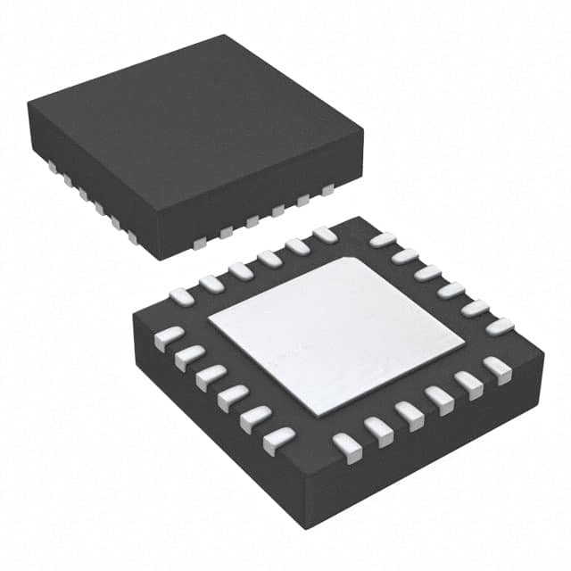
Supplied in a thermally enhanced QFN24 (4 mm × 4 mm, 0.5 mm pitch) package with exposed thermal pad (EP) for PCB heat sinking. Pin 1 marked by dot; pin numbering follows standard counter-clockwise sequence starting from top-left corner.
| Pin/Terminal | Circuit Role | Design Meaning |
|---|---|---|
| VCC | Primary power input | 8–16 V supply for internal logic and gate drivers; UVLO activates below 4.7 V. |
| VOUT | LNB output power rail | Delivers regulated 13/18 V to LNB; carries superimposed 22 kHz tone and DiSEqC data. |
| LX | Boost switch node | Connects to external inductor and Schottky diode/capacitor; switches at ~1 MHz. |
| GND | Power and signal reference | Dual-function ground plane; requires low-impedance connection to EP for thermal performance. |
| SDA / SCL | I²C bidirectional interface | Standard-mode (100 kHz) or fast-mode (400 kHz) communication with host MCU. |
| DSQIN | DiSEqC input control | TTL-compatible pin accepting external 22 kHz tone or DiSEqC envelope for tone activation. |
| DETIN | DiSEqC receive input | AC-coupled pin detecting incoming DiSEqC commands from LNB bus for bi-directional 2.0 support. |
| DSQOUT | DiSEqC data output | Open-drain output providing PWK-encoded DiSEqC response signals to downstream devices. |
| FLT | Fault flag output | Active-low open-drain indicator asserting on OLF, OTF, or PNG faults; requires external pull-up. |
| ISEL | Current limit programming | Resistor-to-GND sets linear regulator current limit from 300 mA to 1 A per ISET bit configuration. |
Key Features
| Feature | Design Value |
|---|---|
| Integrated DiSEqC 2.0 transceiver | Bi-directional command/response via DETIN/DSQOUT with BPSW-controlled RL filter bypass during transmission. |
| Programmable soft-start timing | 4 ms (0→13 V) and 6 ms (0→18 V) - prevents inrush current damage to input capacitors and connectors. |
| Dynamic overload recovery | PCL mode cycles output ON/OFF automatically; OLR bit selects auto-resume (OLR=0) or manual re-enable (OLR=1). |
| Comprehensive diagnostics | 8 real-time I²C status bits with latching behavior - enables remote fault isolation without oscilloscope access. |
| Low-power mode (LPM) | Reduces LDO dropout to 0.6 V and dissipation to 0.3 W @ 500 mA - extends thermal margin in fanless enclosures. |
Applications
| Digital Satellite STB | Hybrid DVB-S2/DVB-T Receiver |
|---|---|
Use Scenario: Integrated satellite tuner module in consumer set-top boxes receiving encrypted broadcast services. IC Role / Device Role / Timing Role: Provides 18 V LNB power, 22 kHz tone for universal LNB switching, and DiSEqC 2.0 command reception from IRD microcontroller. Use Value: Eliminates discrete DC-DC + LDO + tone generator design, reducing BOM count by ≥7 components and PCB area by 35%. |
Use Scenario: Dual-tuner terrestrial/satellite TV receiver requiring independent LNB control per tuner path. IC Role / Device Role / Timing Role: Delivers synchronized 13/18 V outputs with independent I²C addressing (ADDR pin selectable) for multi-LNB configurations. Use Value: Enables simultaneous DiSEqC polling of multiple LNBs while maintaining <1 µs tone enable delay for fast channel switching. |
| PC-Based Satellite Tuner Card | Professional Satellite Monitoring Unit |
Use Scenario: Low-profile PCIe or USB satellite capture card for content acquisition and analysis. IC Role / Device Role / Timing Role: Supplies stable 13 V to LNB under variable host bus power conditions; monitors IMON to detect cable disconnect during hot-plug operation. Use Value: Prevents false LNB failure alarms via 12 mA minimum load detection and automatic FLT assertion on open-circuit events. |
Use Scenario: Field-deployable satellite signal analyzer verifying DiSEqC command integrity and LNB response latency. IC Role / Device Role / Timing Role: Generates calibrated 22 kHz tone with ±1.5% accuracy and validates received DiSEqC envelopes via TMON/TDET diagnostics. Use Value: Replaces external tone generator + scope setup with self-contained validation using I²C register reads and FLT pin state. |
Equivalent & Alternatives
The following parts are listed as comparable options for similar LNB supply and control applications.
| Alternative Part | Technical Difference | Application Difference | Selection Advice |
|---|---|---|---|
| MAX2181AETL+ | Single 13/18 V output; no integrated 22 kHz generator - requires external oscillator or MCU GPIO. | Lacks DiSEqC 2.0 receive (DETIN) and bi-directional DSQOUT; limited to DiSEqC 1.x transmit-only. | Choose when cost sensitivity outweighs DiSEqC 2.0 feature need and board space allows external tone circuitry. |
| LM48530RHBT | Fixed 13/18 V selection via EN1/EN2 pins; no I²C interface - lacks programmable voltage levels and diagnostics. | No register-based fault reporting; relies on discrete comparators and external logic for protection monitoring. | Prefer for ultra-simple STB designs where firmware complexity must be minimized and diagnostic visibility is secondary. |
Compared with MAX2181AETL+ and LM48530RHBT, the LNBH25PQR delivers full DiSEqC 2.0 interoperability, 15-step voltage granularity, and eight-point I²C diagnostics in one QFN24 package - enabling smaller, smarter, and more field-serviceable satellite front-ends.
Availability
LNBH25PQR is available at Aetrix Electronics and suitable for digital satellite STBs, hybrid DVB-S2/DVB-T receivers, PC-based satellite tuner cards, and professional satellite monitoring units requiring stable component supply, long-term lifecycle assurance, and traceable sourcing.
Supply support for LNBH25PQR includes scheduled delivery planning, volume procurement assistance, BOM continuity management, traceable sourcing, and lifecycle availability coordination for OEM customers, industrial embedded developers, connected-device designers, and electronics production programs.
Manufacturer
STMicroelectronics is a global semiconductor leader headquartered in Geneva, Switzerland, designing and manufacturing analog, power, microcontroller, and sensor solutions for automotive, industrial, and consumer markets.
The LNBH25PQR belongs to ST's satellite interface IC product line, engineered specifically to consolidate LNB power, tone generation, DiSEqC control, and diagnostics into a single chip for compact, high-reliability satellite receiver designs.
FAQ
What is the maximum output current capability of the LNBH25PQR?
The LNBH25PQR supports up to 1 A output current, programmable via an external resistor on the ISEL pin. Typical settings include 300 mA (RSEL = 100 kΩ), 500 mA (RSEL = 68 kΩ), and 1 A (RSEL = 33 kΩ), with ±10% tolerance. Current limit is enforced by the integrated linear regulator stage after the boost converter.
How does the LNBH25PQR handle DiSEqC 2.0 bi-directional communication?
It uses DETIN to AC-couple incoming DiSEqC commands from the LNB bus and decodes them internally, making PWK data available on DSQOUT. The BPSW pin controls an external transistor to bypass the output RL filter during transmission, preserving 22 kHz waveform fidelity - a requirement for DiSEqC 2.0 timing compliance.
Can the LNBH25PQR operate with a 12 V only input supply?
Yes - the integrated step-up converter accepts 8–16 V input, making 12 V nominal supply fully compatible. At 12 V input, the boost stage generates ~14.5 V (VUP) to sustain 13 V or 18 V LDO output with sufficient headroom, achieving 93% efficiency at 0.5 A load per datasheet testing.
What happens during thermal shutdown, and how is it signaled?
When junction temperature exceeds 150 °C (typ.), both the boost converter and LDO shut down immediately. The OTF bit in STATUS1 register is latched HIGH, and the open-drain FLT pin is pulled LOW. Operation resumes automatically once temperature falls below 140 °C hysteresis, and OTF clears only after a subsequent I²C status register read.
LNBH25PQR Specifications
- Product attributes
- Attribute value
- Manufacturer:
- STMicroelectronics
- Series:
- -
- Package/Case:
- 24-VFQFN Exposed Pad
- Packaging:
- Tape & Reel (TR)
- Product Status:
- Active
- Applications:
- Converter, Analog and Digital Satellite STB Receivers/SatTV
- Voltage - Input:
- 8V ~ 16V
- Number of Outputs:
- 1
- Voltage - Output:
- 13V, 18.15V
- Operating Temperature:
- 0°C ~ 85°C
- Grade:
- -
- Qualification:
- -
- Mounting Type:
- Surface Mount
- Supplier Device Package:
- 24-QFN (4x4)
LNBH25PQR FAQ
1.How can I place an order for LNBH25PQR through Aetrix?
Please submit a Request for Quotation (RFQ) for LNBH25PQR on Aetrix. Our sales agent will provide a competitive quotation and guide you through the order confirmation once you accept the terms.
2.Are the price and stock information for LNBH25PQR reliable?
The price and inventory of LNBH25PQR are updated periodically and may fluctuate due to market conditions. Stock and pricing data are typically refreshed every 24 hours. Quotation validity for LNBH25PQR is usually 5 days.
3.What payment methods are accepted for LNBH25PQR?
We accept Wire Transfer, PayPal, Credit Card, Western Union, MoneyGram, and Escrow for LNBH25PQR transactions.
Note: Certain payment methods may incur a processing fee.
4.How is shipping managed for LNBH25PQR?
LNBH25PQR orders can be shipped via leading logistics carriers, including DHL, UPS, FedEx, TNT, or Registered Mail.
Once your LNBH25PQR order is processed, you will receive an email with the shipment details and tracking number.
Note: Tracking information may take up to 24 hours to appear. Express delivery typically takes 3–5 business days.
5.How can I obtain technical support or documentation for LNBH25PQR?
For technical support, including LNBH25PQR datasheets, pinout diagrams, or application guidance, please contact our engineering support team. They can provide detailed documentation and assistance for your LNBH25PQR requirements.
6.How does Aetrix verify that LNBH25PQR is sourced from the original manufacturer or authorized distributors?
All LNBH25PQR products on Aetrix are procured from qualified distributors and authorized channels. Our dedicated quality assurance team conducts strict verification, including traceability checks and, if necessary, third-party testing. This ensures that LNBH25PQR meets industry standards.
7.What is the process for return or replacement of LNBH25PQR?
All LNBH25PQR units undergo pre-shipment inspection (PSI). If there is an issue with LNBH25PQR, returns or replacements are accepted under the following conditions:
1.Quantity discrepancies, incorrect items, or visible external defects (such as breakage or corrosion), acknowledged by Aetrix.
2.The issue is reported within 90 days of delivery.
3.The LNBH25PQR part is unused and in its original packaging.
Return procedure for LNBH25PQR:
1.Submit a request within 90 days.
2.Obtain a Return Material Authorization (RMA) from Aetrix.
LNBH25PQR Tags

-
TPS51206DSQR
Texas Instruments

-
TPS51200DRCR
Texas Instruments
-
TPS51200DRCT
Texas Instruments

-
TPS62740DSSR
Texas Instruments

-
TPS51100DGQR
Texas Instruments

-
NCP51200MNTXG
onsemi
-
NCP51400MNTXG
onsemi

-
RT9026GSP
Richtek USA Inc.

-
LP2998MRX/NOPB
Texas Instruments
-
TPS51200QDRCRQ1
Texas Instruments

-
DPA423GN-TL
Power Integrations
-
LM10011SD/NOPB
Texas Instruments
Tech Hub

A practical engineering and sourcing framework covering lifecycle verification, lifetime-buy calculations, replacement qualification, supplier checks and counterfeit-risk controls.

TTL and CMOS logic families differ in thresholds, loading, output drive, power and timing. This engineering guide compares 74HC and 74HCT, calculates noise margins and checks 3.3 V/5 V compatibility.

A practical engineering guide to 3.3V and 5V logic compatibility, input thresholds, resistor dividers, translator ICs, MOSFET level shifting, I2C pull-ups, timing limits and power-sequencing risks.

The 74HC595 uses push-pull logic outputs, while the TPIC6B595 uses 50 V open-drain DMOS sinks for higher-power loads. This guide compares timing, current limits, 3.3 V interfacing, load wiring, thermal…

The 74HC595 converts serial data into eight stable parallel outputs. This guide covers pin functions, shift and storage timing, OE and MR behavior, drive-current limits, cascading, voltage compatibilit…

A technical comparison of level-sensitive latches and edge-triggered flip-flops, covering timing windows, setup and hold limits, master–slave operation, time borrowing, race-through, HDL inference and…

A D latch stores one bit while Enable controls when data can pass. This reference covers gate-level operation, truth tables, transparency, setup and hold timing, LE versus OE, common ICs and practical …

An SR latch stores one bit through cross-coupled feedback. This engineering reference covers NOR and NAND implementations, truth tables, forbidden-state recovery, gated operation, switch debouncing, fa…

Latch circuits retain one bit through feedback. This technical reference covers SR and D latches, truth tables, transparency, timing limits, latch-versus-flip-flop behavior, applications and common log…

An engineering guide to LED driver operation, constant-current and constant-voltage outputs, linear and switching topologies, dimming, IC selection, calculations, replacement compatibility, and fault c…


