
 My Inquiry
 My Account


STMicroelectronics LNBP11SP-TR
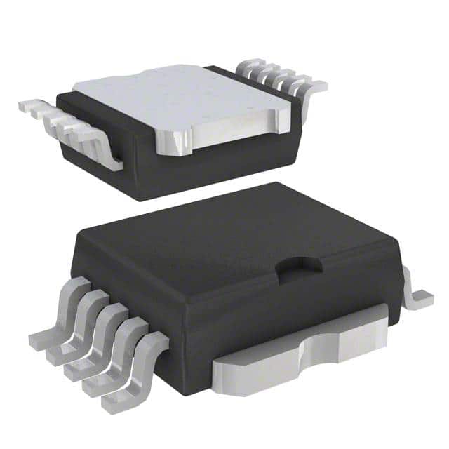
- Part No.:
- LNBP11SP-TR
- Manufacturer:
- STMicroelectronics
- Category:
- Special Purpose Regulators
- Package:
- PowerSO-10 Exposed Bottom Pad
- Datasheet:
-
 LNBP11SP-TR.pdf
- Description:
- IC REG CONV RECVRS 1OUT 10PWRSO
- Quantity:
- Payment:

- Shipping:

Inventory:4,556
Please send an inquiry. Send us your inquiry, and we will respond immediately.
Product details
Overview
LNBP11SP-TR from STMicroelectronics is a monolithic linear LNB power supply and control voltage regulator in PowerSO-10 package, designed to deliver 13 V or 14 V (typ.) output to satellite LNB downconverters via coaxial cable, with logic-selectable port (LNBA), integrated 22 kHz tone oscillator (±2 kHz tolerance), and dynamic overload protection using external 4.7 µF capacitor for 1200 ms cycle time. It supports dual-port satellite receivers requiring remote LNB voltage selection, DiSEqC™ encoding, and cable-length compensation.
For engineers reviewing the LNBP11SP-TR datasheet, LNBP11SP-TR pinout, LNBP11SP-TR application, or LNBP11SP-TR equivalent, key selection criteria include dual-supply input architecture (VCC1/VCC2), 22 kHz tone enable timing, LNB short-circuit diagnostic flag (OLF), bypass functionality for master/slave receiver systems, and thermal shutdown at 150 °C.
Technical Context
The LNBP11SP-TR implements a dual-input linear regulator with automatic VCC1 (15–25 V) or VCC2 (22–25 V) selection based on VSEL/LLC logic states, enabling optimized power dissipation for 13 V or 14 V outputs. Its internal 22 kHz oscillator starts within microseconds to support DiSEqC™ burst coding without external components.
Overcurrent protection operates dynamically: upon detection of overload at LNBA, the output shuts off for tOFF ≈ 1100 ms (with 4.7 µF on CEXT), then resumes briefly for tON = tOFF/15 before rechecking - minimizing thermal stress while maintaining robust start-up into capacitive LNB loads.
Key Specifications
| Parameter | Value and Actual Design Meaning |
|---|---|
| Output Voltage | 13 V (typ.) or 14 V (typ.) selectable via VSEL/LLC logic inputs |
| Tone Frequency | 22 kHz (±2 kHz factory-trimmed) enables DiSEqC™ Level 1.x compliance without calibration |
| Dynamic Overload Cycle | 1200 ms typical total period (tOFF + tON) with 4.7 µF CEXT capacitor |
| Supply Inputs | VCC1: 15–25 V (for 13/14 V outputs); VCC2: 22–25 V (selected automatically) |
| Backward Current Limit | ≤3 mA max when EN = LOW, preventing interference in shared coaxial lines |
| Thermal Shutdown | Triggers at 150 °C junction temperature, protecting against sustained overloads |
| Package | PowerSO-10 surface-mount package with 2.5 K/W thermal resistance (RthJC) |
Pinout & Package
LNBP11SP-TR is housed in a PowerSO-10 package - a thermally enhanced surface-mount outline with exposed die pad for improved heat dissipation, compliant with ECOPACK® lead-free standards and JEDEC JESD97 marking.
| Pin/Terminal | Circuit Role | Design Meaning |
|---|---|---|
| VCC1 | Primary supply input | 15–25 V source used when 13/14 V output selected; lower-voltage rail reduces dissipation |
| VCC2 | Secondary supply input | 22–25 V source automatically engaged for higher-output configurations; supports single-rail operation at 23 V |
| LNBA | Main LNB output port | Delivers regulated 13/14 V to antenna downconverter; routed from MI pin in standby mode |
| VSEL | Voltage selection control | Logic input determining base output: LOW = 13 V, HIGH = 18 V (but LNBP11SP-TR fixed to 13/14 V per truth table) |
| EN | Enable/disable control | LOW disables both outputs and activates 3 mA backward current limit for shared coaxial line safety |
| ENT | Tone oscillator enable | Activates internal 22 kHz square wave (±0.3 Vpp) for DiSEqC™ signaling; fast start-up enables burst coding |
| CEXT | Overload timing capacitor | 4.7 µF sets tOFF ≈ 1100 ms; defines diagnostic cycle duration and thermal duty cycle |
| OLF | Open-collector fault flag | Goes LOW during overload or thermal shutdown; high-impedance otherwise for wired-OR diagnostics |
| EXTM | Analog modulation input | Accepts AC-coupled signals up to 400 mVpp for proprietary LNB control extensions |
| GND | Power and signal reference | Internally connected to die frame; serves as thermal path and return for all regulators and logic |
Key Features
| Feature | Design Value |
|---|---|
| Dual-supply input selection | Automatically switches between VCC1 and VCC2 to minimize power loss at 13/14 V outputs |
| Factory-trimmed 22 kHz oscillator | ±2 kHz accuracy eliminates need for external tuning components or calibration in DiSEqC™ systems |
| Dynamic overload protection | Self-resetting cycle (tOFF/tON) prevents latch-up and limits average power during shorts |
| Standby-mode bypass switch | Routes MI voltage to LNBA when EN = LOW, enabling master/slave coexistence on same coaxial line |
| Cable length compensation | LLC = HIGH adds +1 V to nominal output (13 → 14 V), offsetting coaxial voltage drop |
Applications
| Satellite Receiver Dual-Port Interface | DiSEqC™-Compliant LNB Control |
|---|---|
Use Scenario: Consumer-grade digital satellite receiver with two independent antenna ports feeding separate tuners. IC Role / Device Role / Timing Role: Primary LNB power regulator and control interface IC delivering 13/14 V DC + 22 kHz tone over coaxial cable to each LNB. Use Value: Enables simultaneous reception from two orbital positions using single receiver chassis, with logic-selectable port routing and no external tone generator required. | Use Scenario: Implementation of DiSEqC™ 1.0/1.1 protocols for switching between multiple LNBs or polarization control. IC Role / Device Role / Timing Role: Integrated tone oscillator and fast ENT response provide precise 22 kHz burst modulation synchronized to MCU command timing. Use Value: Eliminates discrete oscillator circuitry and ensures ±2 kHz tone accuracy for reliable DiSEqC™ message decoding by downstream LNBs. |
| Master-Slave Shared Coaxial System | LNB Diagnostic & Protection Interface |
Use Scenario: Single-dish installation where two receivers share one antenna via passive splitter and require coordinated LNB powering. IC Role / Device Role / Timing Role: Slave-mode regulator using MI-to-LNBA bypass switch activated by EN = LOW to defer control to master receiver. Use Value: Prevents conflicting voltage/tone commands on shared coax; backward current limited to ≤3 mA avoids interference with master's regulation. | Use Scenario: Field-deployed satellite terminals requiring fault visibility and thermal resilience under variable environmental loads. IC Role / Device Role / Timing Role: Real-time overload monitor with OLF open-collector flag and self-timed recovery cycle defined by CEXT capacitor. Use Value: Provides unambiguous short-circuit detection and automatic recovery without MCU intervention, reducing firmware complexity and field failure rates. |
Equivalent & Alternatives
The following parts are listed as comparable options for similar LNB supply and control applications.
| Alternative Part | Technical Difference | Application Difference | Selection Advice |
|---|---|---|---|
| LNBP10SP-TR | Fixed 13 V output only; lacks LLC pin and cable-length compensation | Not suitable where coaxial voltage drop exceeds 0.5 V; no +1 V boost capability | Select when system uses short cables (<15 m) and requires lowest BOM cost |
| LNBP12SP-TR | Supports 18 V / 19 V outputs (VSEL=H); different voltage range mapping | Required for universal LNBs needing 18 V vertical / 19 V horizontal polarization | Select when supporting legacy or wide-range LNBs with 18/19 V switching |
Compared with LNBP10SP-TR, LNBP11SP-TR adds cable-length compensation for longer runs; compared with LNBP12SP-TR, it targets 13/14 V-only LNBs common in regional DVB-S deployments, offering tighter regulation and lower thermal load at reduced output voltage.
Availability
LNBP11SP-TR is available at Aetrix Electronics and suitable for satellite receiver design, DiSEqC™-enabled set-top boxes, and professional broadcast equipment requiring stable component supply, consistent 22 kHz tone accuracy, and robust LNB short-circuit protection.
Supply support for LNBP11SP-TR includes scheduled delivery planning, volume procurement assistance, BOM continuity management, traceable sourcing, and lifecycle availability coordination for OEM customers, industrial embedded developers, connected-device designers, and electronics production programs.
Manufacturer
STMicroelectronics is a global semiconductor leader headquartered in Geneva, Switzerland, designing and manufacturing analog, microcontroller, power, and automotive ICs with emphasis on energy efficiency and system integration.
LNBP11SP-TR belongs to the LNBP1X series - a family of monolithic LNB power regulators engineered specifically for cost-sensitive, thermally constrained satellite receiver platforms requiring integrated tone generation, dual-port control, and diagnostic feedback.
FAQ
What is the function of the CEXT pin on LNBP11SP-TR?
The CEXT pin connects an external capacitor (typically 4.7 µF) that sets the OFF time (tOFF ≈ 1100 ms) of the dynamic overload protection circuit. When either LNB output experiences overcurrent, the regulator disables the output for this duration, then briefly resumes for tON = tOFF/15 before rechecking - limiting average power dissipation and enabling safe recovery without manual reset.
Can LNBP11SP-TR drive both LNBA and LNBB simultaneously?
No. LNBP11SP-TR is a PowerSO-10 variant with only one LNB output pin (LNBA); the LNBB pin is omitted per Table 1. It is designed for single-output satellite receivers. For dual-output operation, the PowerSO-20 packaged LNBP20PD-TR or LNBP20CR must be used, which provides dedicated LNBA and LNBB pins with independent control.
How does the LLC pin affect output voltage?
The LLC pin is a logic input that adds +1 V (typ.) to the base output voltage selected by VSEL. With VSEL = LOW (13 V nominal), LLC = HIGH raises output to 14 V (typ.), compensating for coaxial cable voltage drop. This adjustment is implemented internally without external components and is confirmed in the truth table (EN=H, OSEL=L, VSEL=L, LLC=H → VLNBA = 14 V).
Is external decoupling required on the EXTM pin?
Yes. The EXTM pin requires a DC-blocking capacitor (e.g., 100 nF ceramic) between the modulation source and the pin to prevent DC bias from disturbing internal biasing. ST specifies AC coupling for signals up to 400 mVpp; leaving EXTM open is acceptable if external modulation is unused, as the pin has no internal pull-up or pull-down.
LNBP11SP-TR Specifications
- Product attributes
- Attribute value
- Manufacturer:
- STMicroelectronics
- Series:
- -
- Package/Case:
- PowerSO-10 Exposed Bottom Pad
- Packaging:
- Tape & Reel (TR)
- Product Status:
- Obsolete
- Applications:
- Converter, Analog and Digital Satellite Receivers
- Voltage - Input:
- 15V ~ 25V
- Number of Outputs:
- 1
- Voltage - Output:
- 13V, 18V
- Operating Temperature:
- 0°C ~ 85°C
- Grade:
- -
- Qualification:
- -
- Mounting Type:
- Surface Mount
- Supplier Device Package:
- 10-PowerSO
LNBP11SP-TR FAQ
1.How can I place an order for LNBP11SP-TR through Aetrix?
Please submit a Request for Quotation (RFQ) for LNBP11SP-TR on Aetrix. Our sales agent will provide a competitive quotation and guide you through the order confirmation once you accept the terms.
2.Are the price and stock information for LNBP11SP-TR reliable?
The price and inventory of LNBP11SP-TR are updated periodically and may fluctuate due to market conditions. Stock and pricing data are typically refreshed every 24 hours. Quotation validity for LNBP11SP-TR is usually 5 days.
3.What payment methods are accepted for LNBP11SP-TR?
We accept Wire Transfer, PayPal, Credit Card, Western Union, MoneyGram, and Escrow for LNBP11SP-TR transactions.
Note: Certain payment methods may incur a processing fee.
4.How is shipping managed for LNBP11SP-TR?
LNBP11SP-TR orders can be shipped via leading logistics carriers, including DHL, UPS, FedEx, TNT, or Registered Mail.
Once your LNBP11SP-TR order is processed, you will receive an email with the shipment details and tracking number.
Note: Tracking information may take up to 24 hours to appear. Express delivery typically takes 3–5 business days.
5.How can I obtain technical support or documentation for LNBP11SP-TR?
For technical support, including LNBP11SP-TR datasheets, pinout diagrams, or application guidance, please contact our engineering support team. They can provide detailed documentation and assistance for your LNBP11SP-TR requirements.
6.How does Aetrix verify that LNBP11SP-TR is sourced from the original manufacturer or authorized distributors?
All LNBP11SP-TR products on Aetrix are procured from qualified distributors and authorized channels. Our dedicated quality assurance team conducts strict verification, including traceability checks and, if necessary, third-party testing. This ensures that LNBP11SP-TR meets industry standards.
7.What is the process for return or replacement of LNBP11SP-TR?
All LNBP11SP-TR units undergo pre-shipment inspection (PSI). If there is an issue with LNBP11SP-TR, returns or replacements are accepted under the following conditions:
1.Quantity discrepancies, incorrect items, or visible external defects (such as breakage or corrosion), acknowledged by Aetrix.
2.The issue is reported within 90 days of delivery.
3.The LNBP11SP-TR part is unused and in its original packaging.
Return procedure for LNBP11SP-TR:
1.Submit a request within 90 days.
2.Obtain a Return Material Authorization (RMA) from Aetrix.
LNBP11SP-TR Tags

-
TPS51206DSQR
Texas Instruments

-
TPS51200DRCR
Texas Instruments
-
TPS51200DRCT
Texas Instruments

-
TPS62740DSSR
Texas Instruments

-
TPS51100DGQR
Texas Instruments

-
NCP51200MNTXG
onsemi
-
NCP51400MNTXG
onsemi

-
RT9026GSP
Richtek USA Inc.

-
LP2998MRX/NOPB
Texas Instruments
-
TPS51200QDRCRQ1
Texas Instruments

-
DPA423GN-TL
Power Integrations
-
LM10011SD/NOPB
Texas Instruments
Tech Hub

A practical engineering guide to 3.3V and 5V logic compatibility, input thresholds, resistor dividers, translator ICs, MOSFET level shifting, I2C pull-ups, timing limits and power-sequencing risks.

The 74HC595 uses push-pull logic outputs, while the TPIC6B595 uses 50 V open-drain DMOS sinks for higher-power loads. This guide compares timing, current limits, 3.3 V interfacing, load wiring, thermal…

The 74HC595 converts serial data into eight stable parallel outputs. This guide covers pin functions, shift and storage timing, OE and MR behavior, drive-current limits, cascading, voltage compatibilit…

A technical comparison of level-sensitive latches and edge-triggered flip-flops, covering timing windows, setup and hold limits, master–slave operation, time borrowing, race-through, HDL inference and…

A D latch stores one bit while Enable controls when data can pass. This reference covers gate-level operation, truth tables, transparency, setup and hold timing, LE versus OE, common ICs and practical …

An SR latch stores one bit through cross-coupled feedback. This engineering reference covers NOR and NAND implementations, truth tables, forbidden-state recovery, gated operation, switch debouncing, fa…

Latch circuits retain one bit through feedback. This technical reference covers SR and D latches, truth tables, transparency, timing limits, latch-versus-flip-flop behavior, applications and common log…

An engineering guide to LED driver operation, constant-current and constant-voltage outputs, linear and switching topologies, dimming, IC selection, calculations, replacement compatibility, and fault c…

Operational amplifier guide covering op amp basics, feedback, ideal vs real op amps, common configurations, buffer circuits, offset, bias current, gain-bandwidth, slew rate, rail-to-rail limits and sel…

Jumper cables guide covering safe connection order, red and black clamp placement, final ground connection, cable gauge, length, clamp quality, copper vs CCA cables, jump starter comparison and battery…


