
 My Inquiry
 My Account


STMicroelectronics LNBP12SP-TR
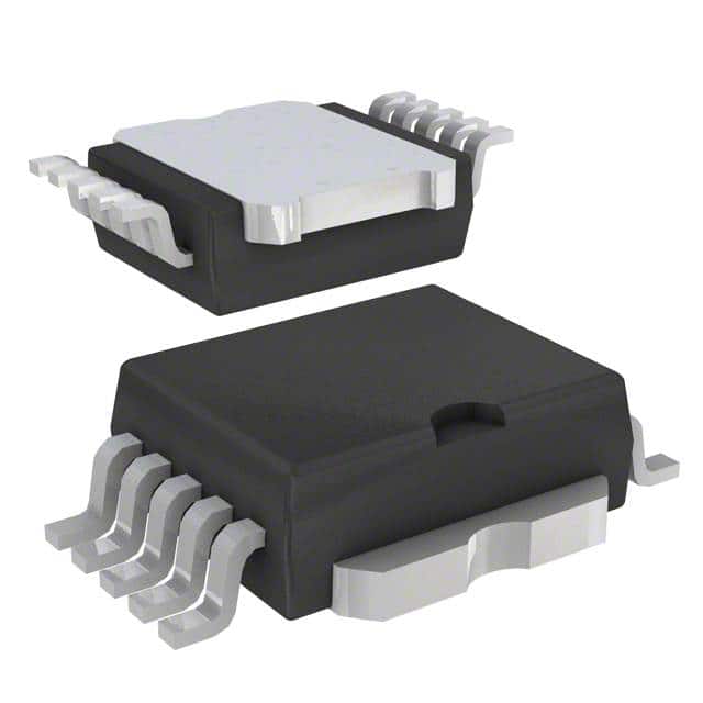
- Part No.:
- LNBP12SP-TR
- Manufacturer:
- STMicroelectronics
- Category:
- Special Purpose Regulators
- Package:
- PowerSO-10 Exposed Bottom Pad
- Datasheet:
-
 LNBP12SP-TR.pdf
- Description:
- IC REG CONV RECVRS 1OUT 10PWRSO
- Quantity:
- Payment:

- Shipping:

Inventory:1,305
Please send an inquiry. Send us your inquiry, and we will respond immediately.
Product details
Overview
LNBP12SP-TR from STMicroelectronics is a monolithic linear voltage regulator in PowerSO-10 package, designed to supply and control LNB downconverters via coaxial cable in satellite receivers. It delivers logic-selectable 13 V or 14 V (typ.) outputs to LNBA port, features factory-trimmed 22 kHz tone oscillator (±2 kHz tolerance), dynamic overload protection with 4.7 µF CEXT, dual supply inputs (VCC1/VCC2), and line-length compensation (LLC) for coaxial drop correction. Used in dual-port analog/digital satellite receivers requiring remote LNB powering and DiSEqC™-compatible tone modulation.
For engineers reviewing the LNBP12SP-TR datasheet, LNBP12SP-TR pinout, LNBP12SP-TR application, or LNBP12SP-TR equivalent, key selection criteria include output voltage selection logic (VSEL/LLC), 22 kHz tone enable timing (ENT), dynamic overcurrent cycle time (toff ≈ 1100 ms), backward current limit (<3 mA in standby), and PowerSO-10 thermal resistance (2 °C/W).
Technical Context
The LNBP12SP-TR implements a dual-input linear regulator architecture with automatic VCC1/VCC2 selection based on output voltage setting: VCC1 (15–25 V) powers 13 V output, VCC2 (22–25 V) powers 14 V output. Its internal 22 kHz oscillator enables DiSEqC™ burst coding via fast ENT pin response and factory-trimmed frequency (20–24 kHz).
Overload protection operates dynamically using external CEXT: short-circuit detection triggers 1100 ms off-time (toff), followed by 73 ms on-time (ton ≈ toff/15), with OLF open-collector flag signaling fault. Standby mode (EN = LOW) disables outputs and limits backward current to ≤3 mA while enabling MI-to-LNBA bypass for slave operation.
Key Specifications
| Parameter | Value and Actual Design Meaning |
|---|---|
| Output Voltage | 13 V (typ.) or 14 V (typ.) selectable via VSEL/LLC logic; compensates coaxial voltage drop with +1 V step. |
| Tone Frequency | 22 kHz (typ.), factory trimmed ±2 kHz; no external components needed for DiSEqC™ tone generation. |
| Dynamic Overload Cycle | toff = 1100 ms, ton = 73 ms (typ.) with 4.7 µF CEXT; reduces power dissipation during sustained short circuit. |
| Backward Current Limit | ≤3 mA max when EN = LOW; prevents reverse feed from shared coaxial lines in multi-receiver systems. |
| Supply Input Range | VCC1: 15–25 V (for 13 V output); VCC2: 22–25 V (for 14 V output); internal switch selects optimal rail. |
| Thermal Protection | Junction shutdown at 150 °C; PowerSO-10 RthJC = 2 °C/W enables stable operation with minimal heatsinking. |
| Logic Input Thresholds | VIL = 0.8 V, VIH = 2.5 V; internal 250 kΩ pull-down resistors simplify MCU interface without external biasing. |
Pinout & Package
LNBP12SP-TR uses the PowerSO-10 surface-mount package (9.4–9.6 mm × 13.8–14.4 mm × 3.7 mm height), optimized for thermal performance (RthJC = 2 °C/W) and space-constrained satellite receiver PCBs.
| Pin | Circuit Role | Design Meaning |
|---|---|---|
| 1 | VCC1 | Primary supply input (15–25 V); selected automatically for 13 V output configuration. |
| 2 | VCC2 | Secondary supply input (22–25 V); selected automatically for 14 V output configuration. |
| 3 | LNBA | Main LNB output port; delivers regulated 13 V or 14 V; connects to MI in standby for slave operation. |
| 4 | VSEL | Voltage select input: LOW = 13 V, HIGH = 14 V (with LLC = LOW/HIGH respectively). |
| 5 | EN | Enable control: LOW disables both outputs and activates MI→LNBA bypass; backward current ≤3 mA. |
| 7 | ENT | Tone enable input: HIGH activates 22 kHz square-wave modulation (±0.3 V, 40–60% duty) on LNBA. |
| 8 | CEXT | Overload timing capacitor connection; 4.7 µF sets 1100 ms off-time and 73 ms on-time cycle. |
| 9 | LLC | Line length compensation: HIGH adds +1 V to selected output (13 → 14 V, 18 → 19 V). |
| 10 | GND | Power and signal reference; internally connected to die frame for low-impedance thermal path. |
Key Features
| Feature | Design Value |
|---|---|
| Dual-supply rail selection | Automatic VCC1/VCC2 switching minimizes power dissipation: 13 V output draws from lower-voltage rail. |
| Factory-trimmed 22 kHz oscillator | ±2 kHz tolerance eliminates calibration components; supports DiSEqC™ burst encoding via fast ENT response. |
| Dynamic overload protection | Self-resetting toff/ton cycle (1100 ms / 73 ms) prevents thermal runaway while maintaining LNB startup capability. |
| Coaxial line-length compensation | LLC pin adds +1 V to output voltage, directly offsetting IR drop across long coaxial runs (up to ~100 m). |
| Slave-mode bypass function | EN = LOW routes MI voltage to LNBA via internal switch, enabling single-dish, dual-receiver sharing of one LNB. |
Applications
| Direct Broadcast Satellite Receiver | Dual-LNB Multi-Switch System |
|---|---|
|
Use Scenario: Consumer-grade satellite set-top box with two independent antenna ports for simultaneous reception of different orbital positions. IC Role / Device Role / Timing Role: Primary LNB power controller delivering 13/14 V to LNBA port; generates 22 kHz tone for polarity switching and DiSEqC™ commands. Use Value: Eliminates need for external tone generator or voltage adjustment circuitry; integrated LLC compensates for 3–5 V coaxial drop in installations up to 30 m. |
Use Scenario: Multi-switch distribution system feeding multiple receivers from four LNBs (e.g., Quattro LNB), where one receiver acts as master controller. IC Role / Device Role / Timing Role: Slave-side LNBP regulating power to local LNB while synchronizing with master's tone and control signals via MI pin. Use Value: EN-driven MI→LNBA bypass allows seamless integration into shared coax infrastructure without additional isolation components. |
| DiSEqC™-Compliant Tuner Module | Compact Satellite Signal Analyzer |
|
Use Scenario: Embedded tuner board in professional broadcast monitoring equipment requiring precise 22 kHz tone timing and voltage stability. IC Role / Device Role / Timing Role: Regulator and tone source with <15 µs tone rise/fall time and ±2 kHz frequency accuracy for compliant DiSEqC™ level 1.0/1.1 signaling. Use Value: Factory-trimmed oscillator ensures interoperability with legacy LNBs without field calibration; fast ENT response enables sub-millisecond tone bursts. |
Use Scenario: Portable field test instrument measuring LNB health, noise figure, and coax continuity in installation and maintenance workflows. IC Role / Device Role / Timing Role: Programmable LNB supply with real-time voltage selection (13/14 V), overload diagnostic (OLF flag), and tone-on-demand for signal tracing. Use Value: OLF open-collector output provides immediate hardware-level fault indication; backward current limiting protects instrument during live coax probing. |
Equivalent & Alternatives
The following parts are listed as comparable options for similar LNB supply and control applications.
| Alternative Part | Technical Difference | Application Difference | Selection Advice |
|---|---|---|---|
| LNBP10SP-TR | Fixed 13 V output only; no LLC pin or line-length compensation; lacks EXTM modulation input. | Suitable for basic single-voltage LNB systems without coax drop compensation requirements. | Select when design uses short coax runs (<15 m) and does not require 14 V output or external modulation. |
| LNBP13SP-TR | Supports 13 V / 14 V outputs but uses PowerSO-10 with MI pin enabled (LNBP12SP-TR omits MI); includes EXTM pin. | Enables master-slave coordination in dual-receiver setups where MI routing is required for bypass. | Choose when system architecture mandates MI-based slave operation or requires analog external modulation capability. |
Compared with LNBP10SP-TR, LNBP12SP-TR adds line-length compensation for longer coax runs; compared with LNBP13SP-TR, it removes MI functionality to reduce pin count while retaining core voltage selection and tone generation-ideal for cost-sensitive, fixed-topology receivers.
Availability
LNBP12SP-TR is available at Aetrix Electronics and suitable for satellite receiver design, LNB power module development, and DiSEqC™-compliant tuner integration requiring stable component supply, consistent thermal performance, and long-term obsolescence management.
Supply support for LNBP12SP-TR includes scheduled delivery planning, volume procurement assistance, BOM continuity management, traceable sourcing, and lifecycle availability coordination for OEM customers, industrial embedded developers, connected-device designers, and electronics production programs.
Manufacturer
STMicroelectronics is a global semiconductor leader headquartered in Geneva, Switzerland, designing and manufacturing analog, power, microcontroller, and sensor solutions for industrial, automotive, and consumer markets.
LNBP12SP-TR belongs to the LNBP1X series-a family of monolithic LNB supply regulators engineered specifically for satellite receiver front-end power and control, emphasizing coaxial compatibility, DiSEqC™ readiness, and thermal robustness in compact packages.
FAQ
What is the purpose of the LLC pin on LNBP12SP-TR?
The LLC (Line Length Compensation) pin adds +1 V to the selected output voltage (e.g., 13 V → 14 V) to counteract voltage drop across long coaxial cables. When LLC = HIGH, the regulator delivers 14 V instead of 13 V under identical VSEL conditions. This feature eliminates external resistor networks or adjustable regulators in installations exceeding 20 m cable length.
How does the dynamic overload protection work without external reset circuitry?
LNBP12SP-TR uses an internal timer controlled by the external CEXT capacitor. During overload, it cycles between 1100 ms off-time (toff) and 73 ms on-time (ton), with OLF flag pulled LOW during toff. No external reset is needed-the IC self-resumes after each toff interval. A 4.7 µF capacitor sets this timing; values outside 3.3–10 µF alter cycle duration predictably per datasheet curves.
Can LNBP12SP-TR be used in a master-slave configuration with another LNBP device?
No-LNBP12SP-TR lacks the MI (Master Input) pin required for slave-mode bypass routing. It supports only standalone or master-only operation. For true master-slave systems, LNBP13SP-TR or LNBP20PD-TR must be used, as they include the MI pin and associated internal switch to route master supply to LNBA during standby.
What is the maximum allowable backward current when EN = LOW?
When EN = LOW, LNBP12SP-TR limits backward current from LNBA/LNBB to GND to ≤3 mA maximum, even if external LNB voltages reach 18 V. This protects the IC and prevents interference in shared coaxial systems. The specification holds across full temperature range (−40 °C to +125 °C) and supply conditions (VCC1/VCC2 floating or at 22 V).
LNBP12SP-TR Specifications
- Product attributes
- Attribute value
- Manufacturer:
- STMicroelectronics
- Series:
- -
- Package/Case:
- PowerSO-10 Exposed Bottom Pad
- Packaging:
- Tape & Reel (TR)
- Product Status:
- Obsolete
- Applications:
- Converter, Analog and Digital Satellite Receivers
- Voltage - Input:
- 15V ~ 25V
- Number of Outputs:
- 1
- Voltage - Output:
- 13V, 18V
- Operating Temperature:
- 0°C ~ 85°C
- Grade:
- -
- Qualification:
- -
- Mounting Type:
- Surface Mount
- Supplier Device Package:
- 10-PowerSO
LNBP12SP-TR FAQ
1.How can I place an order for LNBP12SP-TR through Aetrix?
Please submit a Request for Quotation (RFQ) for LNBP12SP-TR on Aetrix. Our sales agent will provide a competitive quotation and guide you through the order confirmation once you accept the terms.
2.Are the price and stock information for LNBP12SP-TR reliable?
The price and inventory of LNBP12SP-TR are updated periodically and may fluctuate due to market conditions. Stock and pricing data are typically refreshed every 24 hours. Quotation validity for LNBP12SP-TR is usually 5 days.
3.What payment methods are accepted for LNBP12SP-TR?
We accept Wire Transfer, PayPal, Credit Card, Western Union, MoneyGram, and Escrow for LNBP12SP-TR transactions.
Note: Certain payment methods may incur a processing fee.
4.How is shipping managed for LNBP12SP-TR?
LNBP12SP-TR orders can be shipped via leading logistics carriers, including DHL, UPS, FedEx, TNT, or Registered Mail.
Once your LNBP12SP-TR order is processed, you will receive an email with the shipment details and tracking number.
Note: Tracking information may take up to 24 hours to appear. Express delivery typically takes 3–5 business days.
5.How can I obtain technical support or documentation for LNBP12SP-TR?
For technical support, including LNBP12SP-TR datasheets, pinout diagrams, or application guidance, please contact our engineering support team. They can provide detailed documentation and assistance for your LNBP12SP-TR requirements.
6.How does Aetrix verify that LNBP12SP-TR is sourced from the original manufacturer or authorized distributors?
All LNBP12SP-TR products on Aetrix are procured from qualified distributors and authorized channels. Our dedicated quality assurance team conducts strict verification, including traceability checks and, if necessary, third-party testing. This ensures that LNBP12SP-TR meets industry standards.
7.What is the process for return or replacement of LNBP12SP-TR?
All LNBP12SP-TR units undergo pre-shipment inspection (PSI). If there is an issue with LNBP12SP-TR, returns or replacements are accepted under the following conditions:
1.Quantity discrepancies, incorrect items, or visible external defects (such as breakage or corrosion), acknowledged by Aetrix.
2.The issue is reported within 90 days of delivery.
3.The LNBP12SP-TR part is unused and in its original packaging.
Return procedure for LNBP12SP-TR:
1.Submit a request within 90 days.
2.Obtain a Return Material Authorization (RMA) from Aetrix.
LNBP12SP-TR Tags

-
TPS51206DSQR
Texas Instruments

-
TPS51200DRCR
Texas Instruments
-
TPS51200DRCT
Texas Instruments

-
TPS62740DSSR
Texas Instruments

-
TPS51100DGQR
Texas Instruments

-
NCP51200MNTXG
onsemi
-
NCP51400MNTXG
onsemi

-
RT9026GSP
Richtek USA Inc.

-
LP2998MRX/NOPB
Texas Instruments
-
TPS51200QDRCRQ1
Texas Instruments

-
DPA423GN-TL
Power Integrations
-
LM10011SD/NOPB
Texas Instruments
Tech Hub

A practical engineering and sourcing framework covering lifecycle verification, lifetime-buy calculations, replacement qualification, supplier checks and counterfeit-risk controls.

TTL and CMOS logic families differ in thresholds, loading, output drive, power and timing. This engineering guide compares 74HC and 74HCT, calculates noise margins and checks 3.3 V/5 V compatibility.

A practical engineering guide to 3.3V and 5V logic compatibility, input thresholds, resistor dividers, translator ICs, MOSFET level shifting, I2C pull-ups, timing limits and power-sequencing risks.

The 74HC595 uses push-pull logic outputs, while the TPIC6B595 uses 50 V open-drain DMOS sinks for higher-power loads. This guide compares timing, current limits, 3.3 V interfacing, load wiring, thermal…

The 74HC595 converts serial data into eight stable parallel outputs. This guide covers pin functions, shift and storage timing, OE and MR behavior, drive-current limits, cascading, voltage compatibilit…

A technical comparison of level-sensitive latches and edge-triggered flip-flops, covering timing windows, setup and hold limits, master–slave operation, time borrowing, race-through, HDL inference and…

A D latch stores one bit while Enable controls when data can pass. This reference covers gate-level operation, truth tables, transparency, setup and hold timing, LE versus OE, common ICs and practical …

An SR latch stores one bit through cross-coupled feedback. This engineering reference covers NOR and NAND implementations, truth tables, forbidden-state recovery, gated operation, switch debouncing, fa…

Latch circuits retain one bit through feedback. This technical reference covers SR and D latches, truth tables, transparency, timing limits, latch-versus-flip-flop behavior, applications and common log…

An engineering guide to LED driver operation, constant-current and constant-voltage outputs, linear and switching topologies, dimming, IC selection, calculations, replacement compatibility, and fault c…


