
 My Inquiry
 My Account


Texas Instruments LP3873ESX-5.0/NOPB
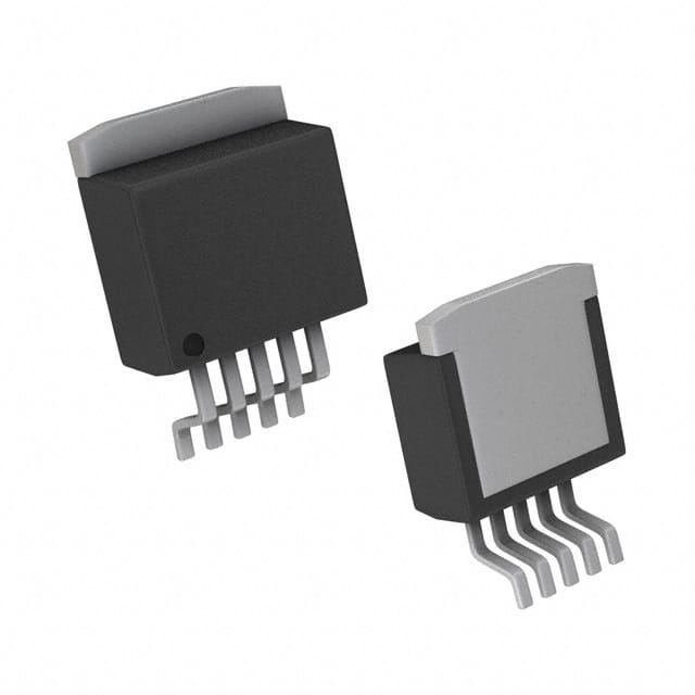
- Part No.:
- LP3873ESX-5.0/NOPB
- Manufacturer:
- Texas Instruments
- Package:
- TO-263-6, D2PAK (5 Leads + Tab), TO-263BA
- Datasheet:
-
 LP3873ESX-5.0/NOPB.pdf
- Description:
- IC REG LIN 5V 3A DDPAK/TO263-5
- Quantity:
- Payment:

- Shipping:

Inventory:1,118
Please send an inquiry. Send us your inquiry, and we will respond immediately.
Product details
Overview
LP3873ESX-5.0/NOPB from Texas Instruments is a 3A ultra-low-dropout linear regulator optimized for microprocessor and DSP power supplies, delivering 5.0V ±1.5% output with 800mV dropout at 3A load, 6mA ground current, and 1µA shutdown quiescent current. It operates from 2.5V–7.0V input and features an open-drain ERROR flag for output monitoring.
For engineers reviewing the LP3873ESX-5.0/NOPB datasheet, LP3873ESX-5.0/NOPB pinout, LP3873ESX-5.0/NOPB application, or LP3873ESX-5.0/NOPB equivalent, key selection criteria include dropout performance under full 3A load, remote-sense capability (not available on LP3873 variant), thermal protection behavior, and minimum output capacitor requirements for stability.
Technical Context
This CMOS-based LDO uses a PMOS pass element to achieve ultra-low dropout-80mV at 300mA and 800mV at 3A-enabling operation with minimal VIN–VOUT margin. Its error amplifier and reference circuitry are designed for fast transient response, critical in low-voltage digital loads where step-load changes exceed 1A/µs.
The device integrates overtemperature and overcurrent protection, with short-circuit limiting set at 6A peak and thermal shutdown activating above +125°C junction temperature. The ERROR flag provides hysteresis (5–8% of VOUT) and resets within 1µs after regulation recovery.
Key Specifications
| Parameter | Value and Actual Design Meaning |
|---|---|
| Output Voltage | 5.0V ±1.5% (room temp), ±3.0% over full line/load/temp range - ensures stable core voltage for 5V-tolerant logic and analog interfaces. |
| Max Output Current | 3A DC continuous - supports high-current FPGA I/O banks or multi-core DSP subsystems without derating at 25°C ambient. |
| Dropout Voltage | 800mV at 3A load - enables use with 5.8V input rails while maintaining 5.0V output, minimizing power loss vs. higher-dropout alternatives. |
| Ground Pin Current | 6mA at 3A load - low bias current preserves efficiency in battery-backed or always-on systems where quiescent loss matters. |
| Shutdown Quiescent Current | 1µA - allows deep sleep mode in portable instrumentation or IoT edge nodes without compromising wake-up latency. |
| Load Regulation | 0.08% - maintains <±4mV output shift across 10mA–3A load range, critical for precision ADC reference or sensor biasing. |
| PSRR @ 120Hz | 73dB (VIN = VOUT +1.0V) - suppresses ripple from upstream switching converters, reducing need for additional filtering stages. |
Pinout & Package
LP3873ESX-5.0/NOPB is packaged in a 5-pin DDPAK/TO-263 surface-mount package with exposed thermal pad (KTT0005B). The package supports high-power dissipation via PCB copper area and is RoHS-compliant and lead-free (NOPB suffix).
| Pin/Terminal | Circuit Role | Design Meaning |
|---|---|---|
| 1 - SD | Shutdown Control Input | CMOS-compatible active-low enable; requires 10kΩ pull-up to VIN if driven by open-collector source; disables regulator and invalidates ERROR flag. |
| 2 - VIN | Main Input Supply | Accepts 2.5V–7.0V; internal parasitic diode allows reverse current up to 200mA DC if VOUT > VIN - must be considered in hot-swap or backup-power designs. |
| 3 - GND | Power Ground Reference | Single-point Kelvin connection required; routing GND traces separately from high-current paths prevents load-regulation errors and instability. |
| 4 - VOUT | Regulated Output Terminal | Delivers 5.0V to load; output capacitor must be placed ≤1 cm away with dedicated low-impedance GND return to ensure stability with ≥10µF/low-ESR ceramic or tantalum. |
| 5 - ERROR | Open-Drain Fault Indicator | Sinks up to 1mA when VOUT drops >10% below nominal; requires external 10kΩ–1MΩ pull-up; disabled during shutdown to minimize leakage. |
Key Features
| Feature | Design Value |
|---|---|
| Ultra-Low Dropout Architecture | 800mV at 3A enables operation from 5.8V input to deliver clean 5.0V - reduces heat generation by ~2.4W vs. 2V-drop competitors at same load. |
| Fast Transient Response | Stabilizes within microseconds after 1A load steps - maintains voltage within ±1% window for microprocessor core domains during burst-mode execution. |
| Integrated Protection | Thermal shutdown + foldback current limiting prevent damage during sustained overload or poor heatsinking - no external components needed. |
| Precision Output Accuracy | ±1.5% at 25°C ensures compatibility with 5V TTL, LVDS, and USB PHY interfaces without post-regulation trimming. |
| Low-Noise Operation | 150µVrms (10Hz–100kHz) output noise - suitable for powering RF synthesizers or high-resolution audio DACs without added LDO filtering. |
Applications
| Microprocessor Power Supplies | GTL/GTL+/SSTL Bus Terminators |
|---|---|
Use Scenario: Providing stable 5.0V supply to Intel Pentium-class CPU I/O buffers or AMD K7/K8 chipset southbridge logic. IC Role / Device Role / Timing Role: Primary post-regulator converting 12V or 5.5V intermediate rail to tightly regulated 5.0V for signal integrity-critical bus drivers. Use Value: 0.08% load regulation holds output within ±4mV across full 10mA–3A dynamic range, preventing GTL+ threshold violations during high-speed data bursts. |
Use Scenario: Biasing termination networks for high-speed parallel buses such as PCI-X or DDR SDRAM command/address lines. IC Role / Device Role / Timing Role: Low-noise, low-impedance 5.0V source for active terminators requiring precise voltage reference and fast current sourcing/sinking. Use Value: 73dB PSRR at 120Hz rejects switching noise from upstream DC/DC converters, eliminating timing jitter on SSTL-2 clock trees. |
| Power Supplies for DSPs | Battery Chargers (Post-Regulation) |
Use Scenario: Delivering clean 5.0V to TI C6000-series DSPs during real-time FFT processing with variable core current draw. IC Role / Device Role / Timing Role: Final-stage regulator decoupling DSP analog I/O and memory interface sections from noisy system power rails. Use Value: 150µVrms broadband noise avoids corruption of 16-bit ADC conversions and preserves SNR in audio codec subsystems. |
Use Scenario: Regulating 5.0V output for USB-powered Li-ion charger ICs (e.g., BQ2407x) where input varies from 5.5V–12V. IC Role / Device Role / Timing Role: Stable voltage reference for charger IC feedback loops, ensuring accurate constant-voltage charge termination. Use Value: ±1.5% initial accuracy and ±3.0% worst-case tolerance guarantee ±150mV compliance with USB BC1.2 5.0V ±5% spec under all operating conditions. |
Equivalent & Alternatives
The following parts are listed as comparable options for similar LDO regulator applications.
| Alternative Part | Technical Difference | Application Difference | Selection Advice |
|---|---|---|---|
| TSS721AIPW | Fixed 5.0V output, 1.5A max, 350mV dropout at 1.5A, SOIC-8 package | Limited to lower current; lacks ERROR flag and shutdown control | Select when board space is constrained and 1.5A suffices; not suitable for 3A microprocessor loads. |
| TPS75733KTTT | 3A, 3.3V fixed output, 150mV dropout at 3A, thermal foldback, 5-pin TO-263 | Different output voltage; superior dropout but incompatible pinout and no ERROR flag | Choose only if system requires 3.3V and lowest possible dropout; requires PCB redesign due to non-pin-compatible layout. |
Compared with LP3873ESX-5.0/NOPB, TSS721AIPW offers smaller footprint but sacrifices 50% current capacity and fault monitoring; TPS75733KTTT delivers better efficiency at 3.3V but cannot replace LP3873ESX-5.0/NOPB without voltage translation or layout revision.
Availability
LP3873ESX-5.0/NOPB is available at Aetrix Electronics and suitable for microprocessor power supplies, GTL/SSTL bus terminators, and DSP power delivery requiring stable component supply, long-term lifecycle support, and traceable manufacturing origin.
Supply support for LP3873ESX-5.0/NOPB includes scheduled delivery planning, volume procurement assistance, BOM continuity management, traceable sourcing, and lifecycle availability coordination for OEM customers, industrial embedded developers, connected-device designers, and electronics production programs.
Manufacturer
Texas Instruments is a global semiconductor leader specializing in analog, embedded processing, and power management technologies, with decades of expertise in high-reliability linear regulators and power delivery ICs.
The LP3873 series belongs to TI's ultra-low-dropout LDO portfolio, engineered specifically for high-current, low-voltage digital systems where transient response, thermal robustness, and output accuracy are critical - including telecom infrastructure, test equipment, and industrial control.
FAQ
What is the maximum input voltage rating for LP3873ESX-5.0/NOPB?
The absolute maximum input voltage for LP3873ESX-5.0/NOPB is +7.5V, but the recommended operating range is 2.5V to 7.0V. Exceeding 7.0V may trigger internal protection circuits or reduce reliability. The minimum input is determined by dropout: for 5.0V output, VIN must be ≥5.8V at 3A load to maintain regulation. Always observe derating curves in the datasheet for elevated temperature operation.
Does LP3873ESX-5.0/NOPB support remote sensing?
No, LP3873ESX-5.0/NOPB does not support remote sensing. That function is exclusive to the LP3876 variant, which substitutes the ERROR pin with a SENSE pin. LP3873ESX-5.0/NOPB regulates voltage at the VOUT pin only; any PCB trace resistance between VOUT and the load introduces proportional IR drop. For remote-load applications, consider LP3876-5.0 or add external compensation circuitry.
What output capacitor is required for stable operation of LP3873ESX-5.0/NOPB?
LP3873ESX-5.0/NOPB requires a minimum 10µF output capacitor with ESR between 10mΩ and 1Ω, placed within 1 cm of the device using dedicated low-impedance traces. Ceramic (X7R/X5R) or solid tantalum capacitors are recommended; aluminum electrolytics are discouraged due to ESR drift at low temperatures. The capacitor must be rated for ≥6.3V and located directly between VOUT and GND pins.
How does the ERROR flag on LP3873ESX-5.0/NOPB behave during shutdown?
When the SD pin is pulled low, the ERROR flag on LP3873ESX-5.0/NOPB is forced invalid and its state becomes undefined - it does not assert or deassert reliably. This is intentional power-saving behavior. To monitor output status during normal operation only, tie SD to VIN via 10kΩ and use the ERROR pin with a compatible pull-up resistor (10kΩ–1MΩ). Do not rely on ERROR during active shutdown.
Is LP3873ESX-5.0/NOPB pin-compatible with other members of the LP3873/LP3876 family?
LP3873ESX-5.0/NOPB shares identical pinout and package (5-pin DDPAK/TO-263) with all LP3873 variants (e.g., LP3873ESX-3.3/NOPB), but is not pin-compatible with LP3876 devices - the LP3876 substitutes the ERROR pin with SENSE. Swapping LP3873ESX-5.0/NOPB for LP3876-5.0 requires PCB modification to reroute the fifth pin function and update external biasing.
LP3873ESX-5.0/NOPB Specifications
- Product attributes
- Attribute value
- Manufacturer:
- Texas Instruments
- Series:
- -
- Package/Case:
- TO-263-6, D2PAK (5 Leads + Tab), TO-263BA
- Packaging:
- Tape & Reel (TR)
- Product Status:
- Active
- Output Configuration:
- Positive
- Output Type:
- Fixed
- Number of Regulators:
- 1
- Voltage - Input (Max):
- 7V
- Voltage - Output (Min/Fixed):
- 5V
- Voltage - Output (Max):
- -
- Voltage Dropout (Max):
- 1.2V @ 3A
- Current - Output:
- 3A
- Current - Quiescent (Iq):
- 9 mA
- Current - Supply (Max):
- 15 mA
- PSRR:
- 73dB ~ 57dB (120Hz)
- Control Features:
- Enable
- Protection Features:
- Over Current, Over Temperature, Short Circuit
- Operating Temperature:
- -40°C ~ 125°C
- Grade:
- -
- Qualification:
- -
- Mounting Type:
- Surface Mount
- Supplier Device Package:
- TO-263 (DDPAK-5)
LP3873ESX-5.0/NOPB FAQ
1.How can I place an order for LP3873ESX-5.0/NOPB through Aetrix?
Please submit a Request for Quotation (RFQ) for LP3873ESX-5.0/NOPB on Aetrix. Our sales agent will provide a competitive quotation and guide you through the order confirmation once you accept the terms.
2.Are the price and stock information for LP3873ESX-5.0/NOPB reliable?
The price and inventory of LP3873ESX-5.0/NOPB are updated periodically and may fluctuate due to market conditions. Stock and pricing data are typically refreshed every 24 hours. Quotation validity for LP3873ESX-5.0/NOPB is usually 5 days.
3.What payment methods are accepted for LP3873ESX-5.0/NOPB?
We accept Wire Transfer, PayPal, Credit Card, Western Union, MoneyGram, and Escrow for LP3873ESX-5.0/NOPB transactions.
Note: Certain payment methods may incur a processing fee.
4.How is shipping managed for LP3873ESX-5.0/NOPB?
LP3873ESX-5.0/NOPB orders can be shipped via leading logistics carriers, including DHL, UPS, FedEx, TNT, or Registered Mail.
Once your LP3873ESX-5.0/NOPB order is processed, you will receive an email with the shipment details and tracking number.
Note: Tracking information may take up to 24 hours to appear. Express delivery typically takes 3–5 business days.
5.How can I obtain technical support or documentation for LP3873ESX-5.0/NOPB?
For technical support, including LP3873ESX-5.0/NOPB datasheets, pinout diagrams, or application guidance, please contact our engineering support team. They can provide detailed documentation and assistance for your LP3873ESX-5.0/NOPB requirements.
6.How does Aetrix verify that LP3873ESX-5.0/NOPB is sourced from the original manufacturer or authorized distributors?
All LP3873ESX-5.0/NOPB products on Aetrix are procured from qualified distributors and authorized channels. Our dedicated quality assurance team conducts strict verification, including traceability checks and, if necessary, third-party testing. This ensures that LP3873ESX-5.0/NOPB meets industry standards.
7.What is the process for return or replacement of LP3873ESX-5.0/NOPB?
All LP3873ESX-5.0/NOPB units undergo pre-shipment inspection (PSI). If there is an issue with LP3873ESX-5.0/NOPB, returns or replacements are accepted under the following conditions:
1.Quantity discrepancies, incorrect items, or visible external defects (such as breakage or corrosion), acknowledged by Aetrix.
2.The issue is reported within 90 days of delivery.
3.The LP3873ESX-5.0/NOPB part is unused and in its original packaging.
Return procedure for LP3873ESX-5.0/NOPB:
1.Submit a request within 90 days.
2.Obtain a Return Material Authorization (RMA) from Aetrix.
LP3873ESX-5.0/NOPB Tags

-
MIC5504-1.8YM5-TR
Microchip Technology
-
MIC5504-3.3YM5-TR
Microchip Technology

-
MIC5365-3.0YC5-TR
Microchip Technology
-
MIC5365-1.8YC5-TR
Microchip Technology
-
MIC5365-2.5YC5-TR
Microchip Technology
-
MIC5365-3.3YC5-TR
Microchip Technology

-
MIC5365-3.3YD5-TR
Microchip Technology

-
MIC5317-3.3YM5-TR
Microchip Technology

-
TLV1117LV33DCYR
Texas Instruments

-
MIC5317-3.3YMT-TZ
Microchip Technology

-
MIC5528-3.3YMT-TR
Microchip Technology

-
TLV75801PDRVR
Texas Instruments
Tech Hub
A D latch stores one bit while Enable controls when data can pass. This reference covers gate-level operation, truth tables, transparency, setup and hold timing, LE versus OE, common ICs and practical …

An SR latch stores one bit through cross-coupled feedback. This engineering reference covers NOR and NAND implementations, truth tables, forbidden-state recovery, gated operation, switch debouncing, fa…

Latch circuits retain one bit through feedback. This technical reference covers SR and D latches, truth tables, transparency, timing limits, latch-versus-flip-flop behavior, applications and common log…

An engineering guide to LED driver operation, constant-current and constant-voltage outputs, linear and switching topologies, dimming, IC selection, calculations, replacement compatibility, and fault c…

Operational amplifier guide covering op amp basics, feedback, ideal vs real op amps, common configurations, buffer circuits, offset, bias current, gain-bandwidth, slew rate, rail-to-rail limits and sel…

Jumper cables guide covering safe connection order, red and black clamp placement, final ground connection, cable gauge, length, clamp quality, copper vs CCA cables, jump starter comparison and battery…

LDO regulator guide covering low dropout voltage, power dissipation, thermal design, PSRR, output noise, capacitor stability, adjustable LDO circuits, LDO vs buck converter and datasheet selection chec…

Conditional Access Module guide covering CAM meaning, CI/CI+ interface, smart card authorization, DVB security workflow, TV and set-top box compatibility, internal electronics, ESD protection, connecto…

Guide to electronic component obsolescence covering EOL risk, PCN/PDN notices, last-time buy planning, replacement options, form-fit-function validation, counterfeit risk and BOM lifecycle management.

18650 battery guide covering lithium-ion cell basics, 3.6V/3.7V voltage, 4.2V charging, mAh and Wh capacity, protected cells, chargers, BMS, series-parallel packs, holders, welding and sourcing checks.…


