
 My Inquiry
 My Account


Texas Instruments LP5523TM/NOPB
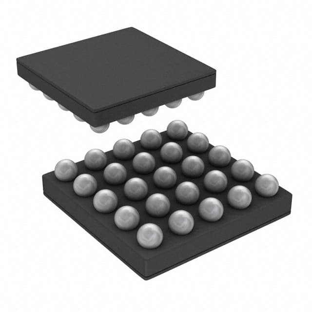
- Part No.:
- LP5523TM/NOPB
- Manufacturer:
- Texas Instruments
- Category:
- LED Drivers
- Package:
- 25-WFBGA, DSBGA
- Datasheet:
-
 LP5523TM/NOPB.pdf
- Description:
- IC LED DRVR RGLTR PWM 25DSBGA
- Quantity:
- Payment:

- Shipping:

Inventory:3,335
Please send an inquiry. Send us your inquiry, and we will respond immediately.
Product details
Overview
LP5523TM/NOPB from Texas Instruments is a nine-channel high-side RGB- and white-LED driver with integrated 1×/1.5× adaptive charge pump, 8-bit current control (25.5 mA full-scale), 12-bit PWM resolution, and on-chip program memory for autonomous lighting effects in mobile devices.
For engineers reviewing the LP5523TM/NOPB datasheet, LP5523TM/NOPB pinout, LP5523TM/NOPB application, or LP5523TM/NOPB equivalent, key selection criteria include charge-pump efficiency up to 94%, 200-nA standby current, I²C-compatible interface with four selectable addresses, built-in LED open/short detection, and temperature-compensated PWM luminance control.
Technical Context
The LP5523TM/NOPB implements three independent programmable execution engines supporting concurrent LED banks-each configurable for keypad illumination, fun lights, or indicator functions-with 96 total instructions stored in internal SRAM. Its adaptive charge pump autonomously selects 1× or 1.5× gain based on forward voltage of D1–D6 outputs, while D7–D9 are directly powered from VDD to bypass the pump for red LED elements.
It integrates a temperature-sensing element enabling linear PWM duty-cycle adjustment across −40°C to +90°C using one of 31 user-selectable slopes; the GPO pin provides digital control signaling, and the INT pin delivers end-of-sequence interrupts to host MCUs. The device supports external 32.7-kHz clock input or internal oscillator operation.
Key Specifications
| Parameter | Value and Actual Design Meaning |
|---|---|
| VDD Range | 2.7 V to 5.5 V - supports full Li-ion battery voltage range without external regulation |
| Max Output Current | 25.5 mA per channel - sufficient to drive standard RGB and WLEDs at full brightness |
| PWM Resolution | 12-bit - enables 4096-step dimming control for smooth lighting transitions |
| Charge Pump Efficiency | Up to 94% - minimizes power loss during voltage boosting for WLEDs |
| Standby Current | 200 nA typical - extends battery life during display-off or idle states |
| LED Matching Error | ±2.5% max - ensures uniform brightness across all nine channels under same programming |
| I²C Speed | 400 kHz Fast Mode - allows rapid configuration and real-time pattern updates |
Pinout & Package
LP5523TM/NOPB uses a 25-pin DSBGA package (2.26 mm × 2.26 mm, 0.4-mm pitch) with exposed thermal pad. All nine LED outputs (D1–D9) are high-side current sources; D7–D9 are internally connected to VDD, while D1–D6 are supplied via the charge pump output (VOUT).
| Pin/Terminal | Circuit Role | Design Meaning |
|---|---|---|
| D1–D6 | High-side current source output | Driven by adaptive charge pump (VOUT); optimized for WLEDs and green/blue LEDs |
| D7–D9 | High-side current source output | Directly powered from VDD; intended for low-VF red LEDs to avoid charge-pump loading |
| VOUT | Charge pump regulated output | Provides 1× or 1.5× boosted voltage (e.g., ~4.5 V at 1.5×) for D1–D6 |
| C1+/C1−, C2+/C2− | Flying capacitor terminals | Interface with two external 0.47 µF ceramic capacitors for charge-pump operation |
| CIN/COUT | Input/output decoupling | 1 µF MLCCs stabilize input and charge-pump output rails |
| SCL/SDA | I²C interface | Two-wire bus with four selectable addresses (via ASEL0/ASEL1) for multi-device systems |
| EN | Enable input | Hardware shutdown control; disables all outputs and reduces supply current to 1 µA |
| INT | Open-drain interrupt | Signals MCU when programmed lighting sequence completes or error occurs |
| GPO | General-purpose output | Configurable digital signal output for synchronizing external peripherals |
| TRIG | Trigger input | Allows hardware synchronization between multiple LP5523TM/NOPB devices |
Key Features
| Feature | Design Value |
|---|---|
| Three independent program engines | Enables concurrent, non-interfering lighting sequences (e.g., breathing + blink + static) across grouped LED banks |
| Built-in LED test circuitry | Detects open/short faults and measures LED forward voltage or VDD/INT pin voltages via I²C register reads |
| Automatic power-save mode | Reduces supply current to 10 µA typical when all outputs are inactive - no software polling required |
| Temperature-compensated PWM | Adjusts luminance in real time using on-die thermal sensor and 31 selectable compensation slopes |
| Source (high-side) drivers | Eliminates need for external high-side FETs; simplifies PCB layout and improves reliability in portable designs |
Applications
| Mobile Keypad Illumination | RGB Status Indicator |
|---|---|
|
Use Scenario: Backlighting alphanumeric keys on smartphones or feature phones with dynamic color feedback. IC Role / Device Role / Timing Role: High-side current source driving three RGB LEDs (D1–D3, D4–D6, D7–D9) with independent 12-bit PWM control per channel. Use Value: Enables smooth color transitions and synchronized animations without MCU intervention, reducing host processor load and power consumption. |
Use Scenario: Visual status indication on wearables or IoT edge nodes using tri-color LED patterns. IC Role / Device Role / Timing Role: Autonomous pattern generator executing preloaded sequences (e.g., heartbeat, pulse) via internal SRAM program memory. Use Value: Delivers consistent, low-power visual feedback even during MCU sleep modes - critical for battery-constrained devices. |
| WLED Backlighting | Haptic-Visual Feedback |
|
Use Scenario: Driving six white LEDs for small-display backlighting in handheld medical or industrial devices. IC Role / Device Role / Timing Role: Adaptive charge pump (1×/1.5×) supplies D1–D6 with regulated voltage across full 2.7–5.5 V input range. Use Value: Maintains >90% efficiency over entire Li-ion discharge curve - eliminates need for external boost converter or LDO. |
Use Scenario: Coordinating tactile vibration and LED flash in gaming controllers or AR interfaces. IC Role / Device Role / Timing Role: GPO pin triggers external haptic driver while INT pin notifies MCU upon LED animation completion. Use Value: Enables precise hardware-level synchronization between visual and tactile events - improves perceived responsiveness and UX fidelity. |
Equivalent & Alternatives
The following parts are listed as comparable options for similar LED driver applications.
| Alternative Part | Technical Difference | Application Difference | Selection Advice |
|---|---|---|---|
| LP55231TM/NOPB | Same pinout and register map; adds enhanced thermal shutdown threshold (150°C vs. 125°C) and improved ESD robustness (±8 kV HBM on D pins) | Preferred for high-reliability consumer or automotive interior lighting where ambient temperature exceeds 85°C | Select LP55231TM/NOPB when extended thermal margin or higher ESD immunity is required; otherwise LP5523TM/NOPB remains optimal for cost-sensitive mobile designs |
| LP5562RTER | 12-channel architecture; supports 1.2-MHz I²C; includes integrated 32-kHz oscillator (no external CLK needed); different DSBGA-30 package | Targeted at next-gen devices requiring more LED channels or simplified clocking; not pin-compatible | Choose LP5562RTER only when expanding beyond nine channels or eliminating external clock components - requires PCB redesign |
Compared with LP5523TM/NOPB, LP55231TM/NOPB offers identical functionality with upgraded protection features, while LP5562RTER provides greater channel count and integration at the cost of package and layout incompatibility - making LP5523TM/NOPB the most balanced choice for established nine-channel RGB/WLED systems.
Availability
LP5523TM/NOPB is available at Aetrix Electronics and suitable for mobile keypad illumination, RGB status indicators, WLED backlighting, and haptic-visual feedback systems requiring stable component supply and long-term production continuity.
Supply support for LP5523TM/NOPB includes scheduled delivery planning, volume procurement assistance, BOM continuity management, traceable sourcing, and lifecycle availability coordination for OEM customers, industrial embedded developers, connected-device designers, and electronics production programs.
Manufacturer
Texas Instruments is a global semiconductor company specializing in analog and embedded processing technologies, with leadership in power management, signal chain, and high-reliability IC design.
The LP5523TM/NOPB belongs to TI's Lighting Management Unit (LMU) product line, engineered specifically for autonomous, low-power LED lighting effects in space-constrained portable electronics - emphasizing efficiency, integration, and firmware-offload capability.
FAQ
What is the primary function of the LP5523TM/NOPB in a mobile system?
The LP5523TM/NOPB serves as a fully integrated nine-channel LED driver that autonomously executes lighting patterns using internal program memory, eliminating continuous MCU involvement. It combines adaptive charge-pump power conversion, high-side current sources, temperature-compensated PWM, and I²C control - all in a 2.26 mm × 2.26 mm DSBGA package. This makes LP5523TM/NOPB ideal for battery-powered devices needing efficient, programmable visual feedback without sacrificing processing resources.
How does the LP5523TM/NOPB manage power efficiency across varying input voltages?
The LP5523TM/NOPB maintains high efficiency by dynamically selecting between 1× and 1.5× charge-pump gain based on the forward voltage requirements of LEDs connected to D1–D6. When input voltage is sufficient (e.g., ≥3.6 V), it operates in 1× mode; below that threshold, it switches to 1.5× mode to sustain LED bias. Meanwhile, D7–D9 are powered directly from VDD - bypassing the pump entirely for red LEDs - achieving up to 94% charge-pump efficiency and 93% overall LED drive efficiency. This architecture ensures LP5523TM/NOPB delivers consistent performance across the full 2.7–5.5 V Li-ion battery range.
Can the LP5523TM/NOPB operate without an external microcontroller after initial setup?
Yes - the LP5523TM/NOPB contains 96-word SRAM-based program memory and three independent execution engines, allowing it to run preloaded lighting sequences autonomously. Once configured via I²C (including pattern definitions, timing, and current settings), the device can execute animations, fades, blinks, or breathing effects without further host interaction. The EN pin enables hardware-controlled wake/sleep, and the INT pin signals sequence completion. This self-contained operation makes LP5523TM/NOPB especially valuable in ultra-low-power or MCU-offload scenarios where LP5523TM/NOPB sustains visual functionality independently.
What protection features does the LP5523TM/NOPB include for LED reliability?
The LP5523TM/NOPB integrates multiple hardware-level protections: overcurrent and short-circuit detection in the charge pump; thermal shutdown at 125°C; built-in LED open/short fault detection with VF measurement capability; and soft-start circuitry to limit inrush current during power-up. Its high-side driver architecture inherently prevents shoot-through, and the 200-nA standby current minimizes battery drain during idle periods. These features collectively ensure robust LED operation in consumer electronics environments - directly contributing to field reliability of LP5523TM/NOPB in production deployments.
Is the LP5523TM/NOPB compatible with standard I²C buses and what address options exist?
Yes - the LP5523TM/NOPB implements a fully compliant two-wire I²C interface supporting Fast Mode (400 kHz). It offers four unique slave addresses selectable via the ASEL0 and ASEL1 pins (00, 01, 10, 11), enabling up to four LP5523TM/NOPB devices on a single bus without address conflict. Level-shifting is not required: logic inputs accept 0.2×VDD to 0.8×VDD thresholds, and SDA is open-drain with 3-mA sink capability. This flexibility simplifies system integration and scalability - particularly important in multi-LED zone architectures where LP5523TM/NOPB devices coordinate via shared I²C and TRIG lines.
LP5523TM/NOPB Specifications
- Product attributes
- Attribute value
- Manufacturer:
- Texas Instruments
- Series:
- -
- Package/Case:
- 25-WFBGA, DSBGA
- Packaging:
- Tape & Reel (TR)
- Product Status:
- Active
- Type:
- DC DC Regulator
- Topology:
- Switched Capacitor (Charge Pump)
- Internal Switch(s):
- Yes
- Number of Outputs:
- 9
- Voltage - Supply (Min):
- 2.7V
- Voltage - Supply (Max):
- 5.5V
- Voltage - Output:
- -
- Current - Output / Channel:
- 25.5mA
- Frequency:
- -
- Dimming:
- PWM
- Applications:
- Backlight
- Operating Temperature:
- -30°C ~ 85°C (TA)
- Grade:
- -
- Qualification:
- -
- Mounting Type:
- Surface Mount
- Supplier Device Package:
- 25-DSBGA
LP5523TM/NOPB FAQ
1.How can I place an order for LP5523TM/NOPB through Aetrix?
Please submit a Request for Quotation (RFQ) for LP5523TM/NOPB on Aetrix. Our sales agent will provide a competitive quotation and guide you through the order confirmation once you accept the terms.
2.Are the price and stock information for LP5523TM/NOPB reliable?
The price and inventory of LP5523TM/NOPB are updated periodically and may fluctuate due to market conditions. Stock and pricing data are typically refreshed every 24 hours. Quotation validity for LP5523TM/NOPB is usually 5 days.
3.What payment methods are accepted for LP5523TM/NOPB?
We accept Wire Transfer, PayPal, Credit Card, Western Union, MoneyGram, and Escrow for LP5523TM/NOPB transactions.
Note: Certain payment methods may incur a processing fee.
4.How is shipping managed for LP5523TM/NOPB?
LP5523TM/NOPB orders can be shipped via leading logistics carriers, including DHL, UPS, FedEx, TNT, or Registered Mail.
Once your LP5523TM/NOPB order is processed, you will receive an email with the shipment details and tracking number.
Note: Tracking information may take up to 24 hours to appear. Express delivery typically takes 3–5 business days.
5.How can I obtain technical support or documentation for LP5523TM/NOPB?
For technical support, including LP5523TM/NOPB datasheets, pinout diagrams, or application guidance, please contact our engineering support team. They can provide detailed documentation and assistance for your LP5523TM/NOPB requirements.
6.How does Aetrix verify that LP5523TM/NOPB is sourced from the original manufacturer or authorized distributors?
All LP5523TM/NOPB products on Aetrix are procured from qualified distributors and authorized channels. Our dedicated quality assurance team conducts strict verification, including traceability checks and, if necessary, third-party testing. This ensures that LP5523TM/NOPB meets industry standards.
7.What is the process for return or replacement of LP5523TM/NOPB?
All LP5523TM/NOPB units undergo pre-shipment inspection (PSI). If there is an issue with LP5523TM/NOPB, returns or replacements are accepted under the following conditions:
1.Quantity discrepancies, incorrect items, or visible external defects (such as breakage or corrosion), acknowledged by Aetrix.
2.The issue is reported within 90 days of delivery.
3.The LP5523TM/NOPB part is unused and in its original packaging.
Return procedure for LP5523TM/NOPB:
1.Submit a request within 90 days.
2.Obtain a Return Material Authorization (RMA) from Aetrix.
LP5523TM/NOPB Tags

-
BCR402RE6327HTSA1
Infineon Technologies

-
BCR430UXTSA2
Infineon Technologies

-
BCR420UE6433HTMA1
Infineon Technologies
-
BCR420UE6327HTSA1
Infineon Technologies
-
BCR421UE6327HTSA1
Infineon Technologies

-
LYT1604D-TL
Power Integrations

-
HV9910CLG-G
Microchip Technology

-
CL2N8-G
Microchip Technology

-
BCR420UW6-7
Diodes Incorporated
-
BCR421UW6-7
Diodes Incorporated

-
BCR420UFD-7
Diodes Incorporated
-
BCR421UFD-7
Diodes Incorporated
Tech Hub

A practical engineering guide to 3.3V and 5V logic compatibility, input thresholds, resistor dividers, translator ICs, MOSFET level shifting, I2C pull-ups, timing limits and power-sequencing risks.

The 74HC595 uses push-pull logic outputs, while the TPIC6B595 uses 50 V open-drain DMOS sinks for higher-power loads. This guide compares timing, current limits, 3.3 V interfacing, load wiring, thermal…

The 74HC595 converts serial data into eight stable parallel outputs. This guide covers pin functions, shift and storage timing, OE and MR behavior, drive-current limits, cascading, voltage compatibilit…

A technical comparison of level-sensitive latches and edge-triggered flip-flops, covering timing windows, setup and hold limits, master–slave operation, time borrowing, race-through, HDL inference and…

A D latch stores one bit while Enable controls when data can pass. This reference covers gate-level operation, truth tables, transparency, setup and hold timing, LE versus OE, common ICs and practical …

An SR latch stores one bit through cross-coupled feedback. This engineering reference covers NOR and NAND implementations, truth tables, forbidden-state recovery, gated operation, switch debouncing, fa…

Latch circuits retain one bit through feedback. This technical reference covers SR and D latches, truth tables, transparency, timing limits, latch-versus-flip-flop behavior, applications and common log…

An engineering guide to LED driver operation, constant-current and constant-voltage outputs, linear and switching topologies, dimming, IC selection, calculations, replacement compatibility, and fault c…

Operational amplifier guide covering op amp basics, feedback, ideal vs real op amps, common configurations, buffer circuits, offset, bias current, gain-bandwidth, slew rate, rail-to-rail limits and sel…

Jumper cables guide covering safe connection order, red and black clamp placement, final ground connection, cable gauge, length, clamp quality, copper vs CCA cables, jump starter comparison and battery…


