
 My Inquiry
 My Account


Texas Instruments LP8727TME/NOPB
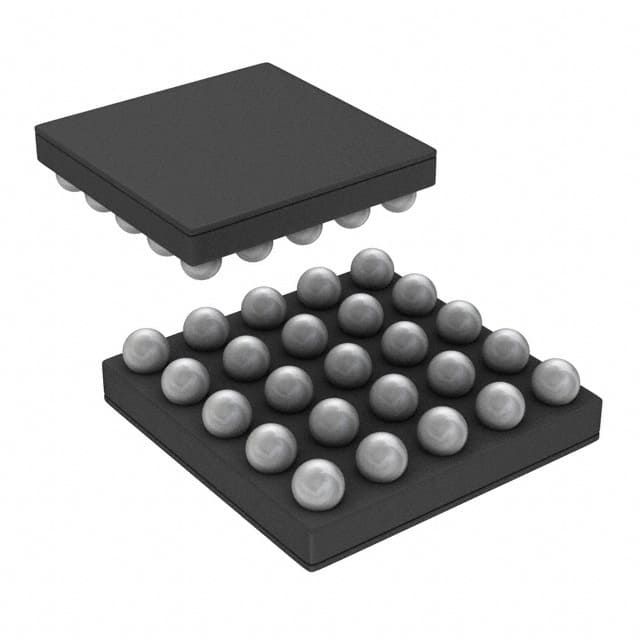
- Part No.:
- LP8727TME/NOPB
- Manufacturer:
- Texas Instruments
- Category:
- Specialized
- Package:
- 25-WFBGA, DSBGA
- Datasheet:
-
 LP8727TME/NOPB.pdf
- Description:
- IC INTFACE SPECIALIZED 25DSBGA
- Quantity:
- Payment:

- Shipping:

Inventory:3,231
Please send an inquiry. Send us your inquiry, and we will respond immediately.
Product details
Overview
LP8727TME/NOPB from Texas Instruments is a highly integrated micro/mini USB interface IC with 28V overvoltage-protected Li-ion charger, dual-path analog switch matrix (USB/UART/audio), and dual LDOs (ID detection & EXPDET). It delivers 400 mA full-rate charging current, supports high-speed USB 2.0 data switching, drives audio inputs to −2.0 V rail, and operates across −40°C to +125°C junction temperature for cellular handset power and connectivity management.
For engineers reviewing the LP8727TME/NOPB datasheet, LP8727TME/NOPB pinout, LP8727TME/NOPB application, or LP8727TME/NOPB equivalent, this device serves as a system-level USB interface, battery charge controller, and analog signal router - requiring attention to I²C register configuration, DSS startup mode selection, thermal regulation limits, and 25-bump thin DSBGA layout constraints.
Technical Context
The LP8727TME/NOPB integrates three functional domains: a 28V OVP single-input linear charger with thermal regulation and programmable 90–1000 mA full-rate current; a configurable analog switch matrix supporting USB DP/DN, UART U1/U2, stereo audio AUD1/AUD2, and MIC paths with charge-pump-enabled negative rail operation; and two independent LDOs - one for ID/SENSE bias (2.3V/2.6V, 1 mA) and one for USB transceiver/PMU wakeup (4.85V, 50 mA, 330 mV dropout).
Switch control is fully I²C-managed (7-bit slave address 0x27), with DSS pin latching default path (USB vs. UART) at first SCL rising edge. All analog switches feature matched on-resistance (≤0.5 Ω mismatch), <360 nA leakage, >107 dB crosstalk suppression, and break-before-make timing. Charger status, VBUS/ID detection, SEND/END button, and microphone removal are reported via interrupt-driven INT\ output and status registers.
Key Specifications
| Parameter | Value and Actual Design Meaning |
|---|---|
| Charging Input OVP | +28 V absolute max; 6.7–7.2 V turn-off threshold protects PMU from transient surges without external clamping. |
| Full-Rate Charge Current | Programmable 90–1000 mA; 400 mA default enables fast Li-ion charging with thermal foldback above 115°C. |
| EXPDET LDO Output | 4.85 V ±3% @ 50 mA; powers USB transceivers or wakes PMU when VBUS is applied. |
| Analog Switch On-Resistance | USB path: 2.5–6 Ω; Audio path: 1.6–3.6 Ω; ensures minimal signal attenuation in high-speed data and audio paths. |
| Operating Temperature | −40°C to +125°C junction range; validated for sustained operation in compact handheld enclosures. |
| I²C Interface | Standard-mode (100 kHz) compatible; 7-bit address 0x27; enables dynamic reconfiguration of switch routing and charger parameters. |
| Package | 25-bump, 0.4 mm pitch thin DSBGA (2.015 mm × 2.015 mm); requires microvia PCB design and controlled reflow profile. |
Pinout & Package
LP8727TME/NOPB uses a 25-bump, 0.4 mm pitch thin DSBGA package (2.015 mm × 2.015 mm) with exposed thermal pad. Pin assignment follows TI's standard top-view layout with five rows (A–E) and five columns (1–5), where GND occupies four bumps (C2, C3, C4, D4) for low-impedance return and thermal dissipation.
| Pin/Terminal | Circuit Role | Design Meaning |
|---|---|---|
| AUD1 (B1) | Stereo audio left input | Analog input pin supporting −2.0 V to +3.6 V range when charge pump enabled; routed to Micro-USB ID jack left channel. |
| D+ (E2), D− (E3) | USB 2.0 differential data I/O | Direct connection to Micro/Mini USB connector D+ and D−; supports high-speed (480 Mbps) signaling with <10 µs turn-on/off. |
| DP (A3), DN (A2) | USB physical layer I/O | Internal USB PHY differential pair; connects to external USB transceiver or processor USB PHY via short trace routing. |
| U1 (A5), U2 (A4) | UART Rx/Tx I/O | Shared pins for UART communication; configured via I²C to route Micro-USB connector to baseband UART instead of USB. |
| ID (E1) | USB accessory identification input | Detects headset insertion via resistor divider; enables SEND/END button and microphone removal interrupts using internal comparators. |
| INT\ (B2) | Open-drain interrupt output | Active-low signal indicating status changes (VBUS detect, charger state, ID event); requires 10 kΩ pull-up for host processor edge-triggered wake-up. |
| SCL/SDA (B4/B3) | I²C serial interface | Configurable control bus; SCL requires 1.5 kΩ pull-up; SDA bidirectional with 1.5 kΩ pull-up; supports register read/write for all functions. |
| VBUS (E4/E5) | USB power input | 28 V tolerant input; powers internal circuits and charger; triggers UVLO (3.5–4.1 V) and OVP (6.7–7.2 V) protection logic. |
| VBAT (C5/D5) | Battery supply input | 2.5–5.5 V input; powers internal LDOs and logic; requires 10 µF ceramic capacitor if no battery present. |
| EXPDET (B5) | Overvoltage-protected LDO output | 4.85 V regulated output; supplies up to 50 mA to USB transceiver or PMU; stable with 1.0 µF ceramic capacitor. |
Key Features
| Feature | Design Value |
|---|---|
| Integrated 28V OVP charger | Eliminates need for external TVS or crowbar circuitry; handles USB wall adapters and automotive USB ports without derating. |
| Charge-pump negative rail generation | Enables −2.0 V audio input swing on AUD1/AUD2, supporting true bipolar headset signals without external op-amps. |
| I²C-configurable switch routing | Allows runtime selection between USB, UART, and audio paths - critical for multi-accessory support in smartphones and tablets. |
| Dual LDO architecture | Separate 2.3/2.6 V ID bias LDO (1 mA) and 4.85 V EXPDET LDO (50 mA) prevent cross-talk and enable independent power domain control. |
| SEND/END & microphone removal detection | On-chip comparators monitor ID pin voltage shifts; generate interrupts for button press and plug/unplug events without host CPU polling. |
| Thermal shutdown with hysteresis | Shuts down at 115°C (typ.), resumes at 130°C; prevents permanent damage during high-current charging in thermally constrained layouts. |
Applications
| Smartphone USB Interface Management | GSM/GPRS/EDGE Handset Power System |
|---|---|
Use Scenario: Managing simultaneous USB data transfer, UART debug access, and stereo headset connection through a single Micro-USB port in space-constrained smartphones. IC Role / Device Role / Timing Role: Analog switch matrix controller and charger supervisor; routes D+/D−, U1/U2, AUD1/AUD2, and MIC based on accessory detection and I²C commands. Use Value: Reduces BOM count by integrating charger, LDOs, and multiplexer - eliminating discrete FETs, level shifters, and protection diodes. |
Use Scenario: Providing robust battery charging and USB peripheral detection in legacy 2G/3G handsets operating under variable input conditions (PC USB, car adapter, wall charger). IC Role / Device Role / Timing Role: 28V-tolerant linear charger with USB IF Rev 1.1 compliance; monitors VBUS, ID, and MIC states to determine charger type and accessory presence. Use Value: Ensures safe charging across unregulated sources; avoids false disconnects during voltage dips via 30–40 mV UVLO hysteresis. |
| Portable Media Player Connectivity Hub | MP3 Player with Headset Detection |
Use Scenario: Enabling USB mass storage mode, firmware update via UART, and line-in recording through shared Micro-USB jack in portable media players. IC Role / Device Role / Timing Role: Dual-path analog switch with I²C arbitration; selects between USB PHY, UART controller, and audio codec based on host command or accessory insertion. Use Value: Supports hot-plug detection and seamless mode switching - e.g., inserting headset disables USB data but enables audio path within <100 µs. |
Use Scenario: Detecting 3-pole vs. 4-pole headset insertion, monitoring SEND/END button presses, and sensing microphone removal in entry-level MP3 players. IC Role / Device Role / Timing Role: ID/SENSE comparator subsystem with 200 kΩ/2.2 kΩ/620 Ω selectable bias; generates INT\ pulses for host MCU on voltage threshold crossings. Use Value: Enables software-defined accessory handling without dedicated GPIOs; reduces firmware complexity via interrupt-driven state machine. |
Equivalent & Alternatives
The following parts are listed as comparable options for similar USB interface and battery charge management applications.
| Alternative Part | Technical Difference | Application Difference | Selection Advice |
|---|---|---|---|
| BQ24075RGTR | Single-function linear charger only; no analog switches, no ID detection, no LDOs; 28V OVP absent (max 20V input). | Used where USB switching and headset detection are handled externally; suitable for simpler power-only designs. | Select when system already implements discrete analog routing and accessory detection; not a functional replacement for LP8727TME/NOPB's integrated features. |
| TUSB1210IRCP | USB 2.0 transceiver with integrated ESD and VBUS detection; no charger, no audio switches, no LDOs; no I²C configurability. | Targets USB PHY layer only; requires separate charger and accessory detection ICs. | Choose for USB-only signal integrity enhancement; cannot replace LP8727TME/NOPB's multi-function integration in handset platforms. |
Compared with BQ24075RGTR and TUSB1210IRCP, LP8727TME/NOPB uniquely combines charger, analog switch matrix, dual LDOs, and intelligent accessory detection in one die - reducing PCB area by >40% and eliminating inter-IC timing coordination overhead in smartphone reference designs.
Availability
LP8727TME/NOPB is available at Aetrix Electronics and suitable for GSM/GPRS/EDGE handsets, portable media players, and MP3 players requiring stable component supply, long-lifecycle support, and production-ready qualification for consumer electronics manufacturing.
Supply support for LP8727TME/NOPB includes scheduled delivery planning, volume procurement assistance, BOM continuity management, traceable sourcing, and lifecycle availability coordination for OEM customers, industrial embedded developers, connected-device designers, and electronics production programs.
Manufacturer
Texas Instruments is a global semiconductor leader specializing in analog, embedded processing, and connectivity solutions for industrial, automotive, and consumer markets.
The LP8727TME/NOPB belongs to TI's Power Management Unit (PMU) portfolio designed specifically for cellular handset and portable media platform integration - merging USB interface, battery charging, and accessory detection into a single compact solution.
FAQ
What is the maximum input voltage tolerance for LP8727TME/NOPB's VBUS pin?
The LP8727TME/NOPB VBUS pin withstands −0.3 V to +28 V per absolute maximum ratings. Its integrated overvoltage protection circuit disables the charger when VBUS exceeds 6.7–7.2 V, safeguarding downstream circuitry without external components. This 28 V rating accommodates automotive USB adapters and transient surges common in handheld environments.
How does LP8727TME/NOPB handle automatic switching between USB and UART modes?
The LP8727TME/NOPB does not auto-switch modes. It latches the DSS pin state at the first SCL rising edge to set default path (USB if DSS low, UART if DSS high), then relies on host processor I²C commands to reconfigure DP/DN, U1/U2, and D+/D− routing. This gives firmware full control over path selection based on detected accessories or user commands.
Can LP8727TME/NOPB support negative-voltage audio signals without external components?
Yes. When CP_EN = 1, LP8727TME/NOPB's internal charge pump enables AUD1 and AUD2 to accept signals from −2.0 V to +3.6 V, allowing direct connection to bipolar headset drivers. No external op-amps or level shifters are needed - the −2.0 V rail is generated on-die and stabilized by internal regulation.
What interrupt sources trigger the INT\ pin on LP8727TME/NOPB?
The INT\ pin asserts low for eight confirmed events: VBUS presence/absence, ID detection state change, SEND/END button press, microphone removal, charger detection completion, thermal shutdown activation, OVLO/UVLO condition, and CHG_STAT transition (pre-charge → CC → CV → EOC). Each source is individually maskable via CONTROL2 register bits.
Is LP8727TME/NOPB pin-compatible with other TI USB interface ICs like LP8732 or LP8758?
No. LP8727TME/NOPB uses a proprietary 25-bump thin DSBGA package with unique pin mapping and functionality. LP8732 is a quad-buck PMU; LP8758 is a 6-phase buck controller - neither integrates analog switches, ID detection, or 28V OVP charging. Direct replacement is not feasible; migration requires full schematic and layout redesign.
LP8727TME/NOPB Specifications
- Product attributes
- Attribute value
- Manufacturer:
- Texas Instruments
- Series:
- -
- Package/Case:
- 25-WFBGA, DSBGA
- Packaging:
- Tape & Reel (TR)
- Product Status:
- Obsolete
- Applications:
- MP3 Players, Portable Media Players
- Interface:
- Micro-USB
- Voltage - Supply:
- -
- Supplier Device Package:
- 25-DSBGA
- Grade:
- -
- Qualification:
- -
- Mounting Type:
- Surface Mount
LP8727TME/NOPB FAQ
1.How can I place an order for LP8727TME/NOPB through Aetrix?
Please submit a Request for Quotation (RFQ) for LP8727TME/NOPB on Aetrix. Our sales agent will provide a competitive quotation and guide you through the order confirmation once you accept the terms.
2.Are the price and stock information for LP8727TME/NOPB reliable?
The price and inventory of LP8727TME/NOPB are updated periodically and may fluctuate due to market conditions. Stock and pricing data are typically refreshed every 24 hours. Quotation validity for LP8727TME/NOPB is usually 5 days.
3.What payment methods are accepted for LP8727TME/NOPB?
We accept Wire Transfer, PayPal, Credit Card, Western Union, MoneyGram, and Escrow for LP8727TME/NOPB transactions.
Note: Certain payment methods may incur a processing fee.
4.How is shipping managed for LP8727TME/NOPB?
LP8727TME/NOPB orders can be shipped via leading logistics carriers, including DHL, UPS, FedEx, TNT, or Registered Mail.
Once your LP8727TME/NOPB order is processed, you will receive an email with the shipment details and tracking number.
Note: Tracking information may take up to 24 hours to appear. Express delivery typically takes 3–5 business days.
5.How can I obtain technical support or documentation for LP8727TME/NOPB?
For technical support, including LP8727TME/NOPB datasheets, pinout diagrams, or application guidance, please contact our engineering support team. They can provide detailed documentation and assistance for your LP8727TME/NOPB requirements.
6.How does Aetrix verify that LP8727TME/NOPB is sourced from the original manufacturer or authorized distributors?
All LP8727TME/NOPB products on Aetrix are procured from qualified distributors and authorized channels. Our dedicated quality assurance team conducts strict verification, including traceability checks and, if necessary, third-party testing. This ensures that LP8727TME/NOPB meets industry standards.
7.What is the process for return or replacement of LP8727TME/NOPB?
All LP8727TME/NOPB units undergo pre-shipment inspection (PSI). If there is an issue with LP8727TME/NOPB, returns or replacements are accepted under the following conditions:
1.Quantity discrepancies, incorrect items, or visible external defects (such as breakage or corrosion), acknowledged by Aetrix.
2.The issue is reported within 90 days of delivery.
3.The LP8727TME/NOPB part is unused and in its original packaging.
Return procedure for LP8727TME/NOPB:
1.Submit a request within 90 days.
2.Obtain a Return Material Authorization (RMA) from Aetrix.
LP8727TME/NOPB Tags

-
NVT4857UKAZ
NXP Semiconductors

-
TCA8418RTWR
Texas Instruments

-
PCA9546APWR
Texas Instruments

-
MD0100N8-G
Microchip Technology

-
PCA9548APW,118
NXP Semiconductors

-
PCA9540BDP,118
NXP Semiconductors

-
PCA9548APWR
Texas Instruments

-
PCA9546APW,118
NXP Semiconductors

-
PTN3360DBS,518
NXP Semiconductors

-
PCA9546ABS,118
NXP Semiconductors

-
PCA9518PWR
Texas Instruments

-
PCA9545APW,118
NXP Semiconductors
Tech Hub

A practical engineering guide to 3.3V and 5V logic compatibility, input thresholds, resistor dividers, translator ICs, MOSFET level shifting, I2C pull-ups, timing limits and power-sequencing risks.

The 74HC595 uses push-pull logic outputs, while the TPIC6B595 uses 50 V open-drain DMOS sinks for higher-power loads. This guide compares timing, current limits, 3.3 V interfacing, load wiring, thermal…

The 74HC595 converts serial data into eight stable parallel outputs. This guide covers pin functions, shift and storage timing, OE and MR behavior, drive-current limits, cascading, voltage compatibilit…

A technical comparison of level-sensitive latches and edge-triggered flip-flops, covering timing windows, setup and hold limits, master–slave operation, time borrowing, race-through, HDL inference and…

A D latch stores one bit while Enable controls when data can pass. This reference covers gate-level operation, truth tables, transparency, setup and hold timing, LE versus OE, common ICs and practical …

An SR latch stores one bit through cross-coupled feedback. This engineering reference covers NOR and NAND implementations, truth tables, forbidden-state recovery, gated operation, switch debouncing, fa…

Latch circuits retain one bit through feedback. This technical reference covers SR and D latches, truth tables, transparency, timing limits, latch-versus-flip-flop behavior, applications and common log…

An engineering guide to LED driver operation, constant-current and constant-voltage outputs, linear and switching topologies, dimming, IC selection, calculations, replacement compatibility, and fault c…

Operational amplifier guide covering op amp basics, feedback, ideal vs real op amps, common configurations, buffer circuits, offset, bias current, gain-bandwidth, slew rate, rail-to-rail limits and sel…

Jumper cables guide covering safe connection order, red and black clamp placement, final ground connection, cable gauge, length, clamp quality, copper vs CCA cables, jump starter comparison and battery…


