
 My Inquiry
 My Account


NXP Semiconductors LPC8N04FHI24E
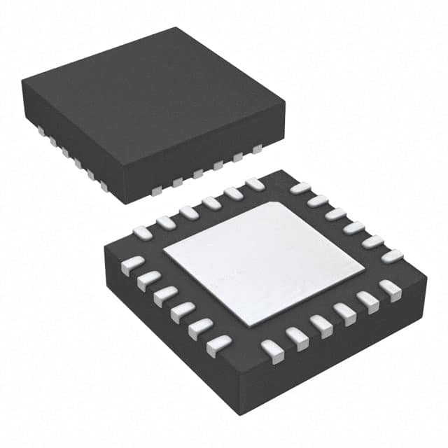
- Part No.:
- LPC8N04FHI24E
- Manufacturer:
- NXP Semiconductors
- Category:
- Microcontrollers
- Package:
- 24-VFQFN Exposed Pad
- Datasheet:
-
 LPC8N04FHI24E.pdf
- Description:
- IC MCU 32BIT 32KB FLASH 24HVQFN
- Quantity:
- Payment:

- Shipping:

Inventory:305
Please send an inquiry. Send us your inquiry, and we will respond immediately.
Product details
Overview
LPC8N04FHI24E from NXP Semiconductors is a 32-bit ARM Cortex-M0+ microcontroller with integrated NFC/RFID ISO 14443 Type A interface, 32 kB flash, 8 kB SRAM, and ultra-low-power operation down to <50 nA in battery-off mode. It supports energy harvesting from NFC fields, OTA firmware updates via NFC, and operates across 1.72 V–3.6 V supply or passive NFC power-enabling contactless smart locks, diagnostic tags, and configurable LED systems.
For engineers reviewing the LPC8N04FHI24E datasheet, LPC8N04FHI24E pinout, LPC8N04FHI24E application, or LPC8N04FHI24E equivalent, key selection considerations include NFC field-powered wake-up capability, 12 GPIO pins with high-current drive (20 mA), SWD debug support, temperature sensor accuracy (±1.5 °C), and deep power-down mode with external wake-up via PIO0_0.
Technical Context
The LPC8N04FHI24E integrates an ARM Cortex-M0+ core with Nested Vectored Interrupt Controller (NVIC), Serial Wire Debug (SWD), and system tick timer-running at up to 8 MHz from an internal 8 MHz FRO trimmed to ±2%. Its clock architecture includes a dedicated 32.768 kHz timer oscillator for RTC and independent power domains managed by the PMU.
Power management is implemented through a dual-source architecture: automatic switching between VDDBAT (1.72–3.6 V) and NFC-harvested power (VNFC), with five operational modes (active, sleep, deep sleep, deep power-down, battery off). The PMU enables power gating per analog peripheral and retains data in five GPREGs during deep power-down.
Key Specifications
| Parameter | Value and Actual Design Meaning |
|---|---|
| CPU Core | ARM Cortex-M0+, up to 8 MHz - enables deterministic real-time control with low gate count and minimal memory footprint |
| Memory | 32 kB flash + 8 kB SRAM + 4 kB EEPROM - supports secure OTA updates, parameter storage, and runtime code execution without external memory |
| NFC Interface | ISO 14443 Type A compliant - enables contactless communication, field-powered wake-up, and encrypted firmware download without battery dependency |
| Power Modes | Five modes including battery-off (<50 nA @ 3.0 V) - extends shelf life for unpowered NFC tags and eliminates battery leakage concerns |
| I/O Capability | 12 GPIO pins; four with 20 mA high-drive; I²C-bus (400 kbit/s); SWD debug - simplifies board design with minimal external components for sensor, LED, or actuator interfacing |
| Temperature Sensor | On-die sensor with ±1.5 °C accuracy (−40 °C to +85 °C) - provides reliable thermal monitoring without calibration or external IC |
| Supply Range | 1.72 V–3.6 V or NFC-field powered - allows flexible deployment in battery-constrained or maintenance-free environments |
Pinout & Package
The LPC8N04FHI24E is housed in a 4 mm × 4 mm × 0.85 mm HVQFN24 (SOT616-3) package with exposed thermal pad. Pin 1 index is marked on top-side; pads 17–18 and 21–24 are reserved; pads 19 (LA) and 20 (LB) serve as NFC antenna terminals.
| Pin/Terminal | Circuit Role | Design Meaning |
|---|---|---|
| 1 (PIO0_0/WAKEUP) | GPIO / Deep power-down wake-up input | Enables field-triggered activation from NFC or external signal; must be pulled HIGH before deep power-down entry |
| 7 (VDDBAT) | Main power supply input | Accepts 1.72–3.6 V; powers digital/analog domains when active; prioritized over NFC power if both present |
| 8 (VSS) | Ground reference | System ground for all domains; must be connected to PCB ground plane for EMI and power integrity |
| 9 (RESETN) | Active-low reset input | Resets CPU, peripherals, and I/O to default states; features weak pull-up to VDDBAT |
| 11 (PIO0_4/SCL) | I²C-bus clock line | Open-drain capable; supports standard/fast mode (100/400 kbit/s); programmable glitch filter |
| 12 (PIO0_5/SDA) | I²C-bus data line | Open-drain capable; supports multi-address recognition and monitor mode for bus diagnostics |
| 15 (PIO0_10/SWCLK) | SWD clock input | Enables ARM Serial Wire Debug; used with PIO0_11 (SWDIO) for programming and real-time debugging |
| 19 (LA) & 20 (LB) | NFC antenna terminals | Differential connection points for external loop antenna; require impedance-matched layout per AN11707 |
Key Features
| Feature | Design Value |
|---|---|
| Energy harvesting from NFC field | Enables full device operation-including wake-up, sensing, and communication-without battery, ideal for disposable or sealed applications |
| OTA firmware update via NFC | Uses Secondary Bootloader (SBL) library in Boot ROM v0.14 to deliver encrypted firmware patches over air, eliminating physical access requirements |
| Ultra-low-power battery-off mode | Consumes <50 nA at 3.0 V with all clocks and domains disabled-preserves battery life for years in storage or standby |
| Programmable high-current GPIO | Four GPIO pins (PIO0_3/7/10/11) deliver 20 mA source/sink-directly drives LEDs, small relays, or logic-level MOSFETs without external drivers |
| Integrated temperature sensor | Provides calibrated on-die measurement (±1.5 °C) across −40 °C to +85 °C-replaces discrete sensors in thermal monitoring and compensation circuits |
Applications
| Configurable LED Strip Control | Smart Toy Data Logger |
|---|---|
Use Scenario: NFC-enabled holiday lighting where users tap a smartphone to change color patterns or brightness. IC Role / Device Role / Timing Role: MCU executes LED control algorithms, stores user preferences in EEPROM, and communicates via NFC ISO 14443 Type A. Use Value: Eliminates buttons and wiring; leverages field power for instant wake-up and configuration-no battery drain during idle periods. | Use Scenario: Embedded in a child's interactive robot to record motion events, ambient temperature, and play duration. IC Role / Device Role / Timing Role: Acts as autonomous data acquisition node-samples temperature sensor, logs timestamps via RTC, and stores data in SRAM/EEPROM. Use Value: Enables post-play analysis via NFC readout; deep power-down mode preserves battery between sessions. |
| Contactless Diagnostic Tag | NFC e-Locker Access Control |
Use Scenario: Adhesive tag on industrial equipment storing calibration history, service intervals, and fault logs. IC Role / Device Role / Timing Role: Serves as secure, tamper-resistant memory and event logger-reads/writes via NFC; uses WDT for reliability. Use Value: Field technicians retrieve full service history with one tap; no connectors or batteries required-ideal for harsh environments. | Use Scenario: Lock mechanism in shared office cabinets activated only upon valid NFC credential presentation. IC Role / Device Role / Timing Role: Authenticates commands via NFC, verifies encryption keys in flash, and triggers solenoid driver via high-current GPIO. Use Value: Zero-power standby until NFC field arrives; battery-off mode ensures multi-year shelf life; OTA updates enable security patching. |
Equivalent & Alternatives
The following parts are listed as comparable options for similar NFC-enabled microcontroller applications.
| Alternative Part | Technical Difference | Application Difference | Selection Advice |
|---|---|---|---|
| ST25DV04K | Dedicated NFC EEPROM (no MCU core); 4 kbit memory; no processing capability or GPIO | Suitable only for passive data storage-not for firmware execution, sensor reading, or actuator control | Select when only NFC-accessible nonvolatile storage is needed; not a functional replacement for LPC8N04FHI24E |
| PN7150B | NFC controller IC with host interface (I²C); no embedded flash/SRAM or ARM core; requires external MCU | Used in host-controlled NFC systems (e.g., with ESP32 or STM32); adds complexity and BOM cost | Choose when higher NFC throughput or advanced protocol support (e.g., peer-to-peer) is required, and a separate MCU is already present |
Compared with ST25DV04K and PN7150B, the LPC8N04FHI24E uniquely integrates NFC interface, ARM Cortex-M0+ processing, and ultra-low-power operation in a single chip-eliminating external controllers, reducing PCB area, and enabling true standalone NFC edge nodes.
Availability
LPC8N04FHI24E is available at Aetrix Electronics and suitable for contactless diagnostic tags, NFC e-lockers, and smart manufacturing identifiers requiring stable component supply, long-term lifecycle assurance, and consistent parametric performance.
Supply support for LPC8N04FHI24E includes scheduled delivery planning, volume procurement assistance, BOM continuity management, traceable sourcing, and lifecycle availability coordination for OEM customers, industrial embedded developers, connected-device designers, and electronics production programs.
Manufacturer
NXP Semiconductors is a global semiconductor leader specializing in secure connectivity solutions for automotive, industrial, and IoT applications-with expertise in ARM-based microcontrollers and NFC technology.
The LPC8N04FHI24E belongs to NXP's LPC800N family of ultra-low-power NFC microcontrollers, designed specifically for battery-free or maintenance-free contactless edge devices in consumer, medical, and industrial settings.
FAQ
What is the maximum system clock frequency supported by the LPC8N04FHI24E?
The LPC8N04FHI24E supports a maximum system clock frequency of 8 MHz, derived from its internal 8 MHz factory-trimmed free-running oscillator (FRO) with ±2% accuracy. Lower frequencies (4 MHz, 2 MHz, etc.) are selectable via clock divider registers-though some peripherals may be disabled at reduced speeds. This 8 MHz limit balances performance, power efficiency, and die size for NFC-centric applications.
Does the LPC8N04FHI24E support Over-the-Air (OTA) firmware updates?
Yes, the LPC8N04FHI24E supports encrypted OTA firmware updates using the Secondary Bootloader (SBL) library stored in Boot ROM version 0.14. Updates are delivered via NFC ISO 14443 Type A interface, enabling field reprogramming without physical access or debug interfaces. The SBL validates firmware signatures and writes to flash memory while preserving critical configuration data in EEPROM.
How does the LPC8N04FHI24E achieve ultra-low power consumption in battery-off mode?
The LPC8N04FHI24E achieves <50 nA current consumption in battery-off mode by disabling all clocks, power domains (VDD1V2, VDD1V6), and analog peripherals while retaining state in the always-on VDD_ALON domain. The PMU cuts power to LDOs and digital logic; only the trigger detector and Brown-Out Detection circuit remain active-ensuring multi-year shelf life for unpowered NFC tags.
Can the LPC8N04FHI24E operate without an external battery?
Yes, the LPC8N04FHI24E can operate entirely from NFC field power via its LA/LB antenna terminals. When powered this way, it supports full functionality-including wake-up, temperature sensing, GPIO control, and NFC communication-at up to 2 MHz system clock. Energy harvesting enables zero-battery designs for disposable or sealed applications like smart labels and diagnostic tags.
What debug interface does the LPC8N04FHI24E provide?
The LPC8N04FHI24E provides ARM Serial Wire Debug (SWD) via pins PIO0_10 (SWCLK) and PIO0_11 (SWDIO). This two-pin interface supports full programming, real-time debugging, breakpoint setting, and memory inspection using standard ARM tools (e.g., Keil MDK, Segger J-Link, OpenOCD). SWD operates independently of NFC or I²C functions and remains accessible even in low-power modes with debug enabled.
LPC8N04FHI24E Specifications
- Product attributes
- Attribute value
- Manufacturer:
- NXP Semiconductors
- Package/Case:
- 24-VFQFN Exposed Pad
- Series:
- LPC8Nxx
- Packaging:
- Tray
- Product Status:
- Active
- Programmable:
- Not Verified
- Core Processor:
- ARM® Cortex®-M0+
- Core Size:
- 32-Bit Single-Core
- Speed:
- 8MHz
- Connectivity:
- I2C, SPI
- Peripherals:
- Brown-out Detect/Reset, POR, PWM, WDT
- Number of I/O:
- 12
- Program Memory Size:
- 32KB (32K x 8)
- Program Memory Type:
- FLASH
- EEPROM Size:
- 4K x 8
- RAM Size:
- 8K x 8
- Voltage - Supply (Vcc/Vdd):
- 1.72V ~ 3.6V
- Data Converters:
- -
- Oscillator Type:
- Internal
- Operating Temperature:
- -40°C ~ 85°C (TA)
- Grade:
- -
- Qualification:
- -
- Mounting Type:
- Surface Mount
- Supplier Device Package:
LPC8N04FHI24E FAQ
1.How can I place an order for LPC8N04FHI24E through Aetrix?
Please submit a Request for Quotation (RFQ) for LPC8N04FHI24E on Aetrix. Our sales agent will provide a competitive quotation and guide you through the order confirmation once you accept the terms.
2.Are the price and stock information for LPC8N04FHI24E reliable?
The price and inventory of LPC8N04FHI24E are updated periodically and may fluctuate due to market conditions. Stock and pricing data are typically refreshed every 24 hours. Quotation validity for LPC8N04FHI24E is usually 5 days.
3.What payment methods are accepted for LPC8N04FHI24E?
We accept Wire Transfer, PayPal, Credit Card, Western Union, MoneyGram, and Escrow for LPC8N04FHI24E transactions.
Note: Certain payment methods may incur a processing fee.
4.How is shipping managed for LPC8N04FHI24E?
LPC8N04FHI24E orders can be shipped via leading logistics carriers, including DHL, UPS, FedEx, TNT, or Registered Mail.
Once your LPC8N04FHI24E order is processed, you will receive an email with the shipment details and tracking number.
Note: Tracking information may take up to 24 hours to appear. Express delivery typically takes 3–5 business days.
5.How can I obtain technical support or documentation for LPC8N04FHI24E?
For technical support, including LPC8N04FHI24E datasheets, pinout diagrams, or application guidance, please contact our engineering support team. They can provide detailed documentation and assistance for your LPC8N04FHI24E requirements.
6.How does Aetrix verify that LPC8N04FHI24E is sourced from the original manufacturer or authorized distributors?
All LPC8N04FHI24E products on Aetrix are procured from qualified distributors and authorized channels. Our dedicated quality assurance team conducts strict verification, including traceability checks and, if necessary, third-party testing. This ensures that LPC8N04FHI24E meets industry standards.
7.What is the process for return or replacement of LPC8N04FHI24E?
All LPC8N04FHI24E units undergo pre-shipment inspection (PSI). If there is an issue with LPC8N04FHI24E, returns or replacements are accepted under the following conditions:
1.Quantity discrepancies, incorrect items, or visible external defects (such as breakage or corrosion), acknowledged by Aetrix.
2.The issue is reported within 90 days of delivery.
3.The LPC8N04FHI24E part is unused and in its original packaging.
Return procedure for LPC8N04FHI24E:
1.Submit a request within 90 days.
2.Obtain a Return Material Authorization (RMA) from Aetrix.
LPC8N04FHI24E Tags

-
ATTINY4-TSHR
Microchip Technology
-
ATTINY10-TSHR
Microchip Technology
-
ATTINY10-TS8R
Microchip Technology

-
ATTINY202-SSNR
Microchip Technology
-
ATTINY202-SSFR
Microchip Technology
-
ATTINY402-SSNR
Microchip Technology

-
PIC16F15213T-I/MF
Microchip Technology
-
PIC16F15213-E/MF
Microchip Technology

-
PIC10F200T-I/OT
Microchip Technology
-
ATTINY412-SSNR
Microchip Technology
-
PIC10F202T-I/OT
Microchip Technology

-
ATTINY404-SSNR
Microchip Technology
Tech Hub

A practical engineering guide to 3.3V and 5V logic compatibility, input thresholds, resistor dividers, translator ICs, MOSFET level shifting, I2C pull-ups, timing limits and power-sequencing risks.

The 74HC595 uses push-pull logic outputs, while the TPIC6B595 uses 50 V open-drain DMOS sinks for higher-power loads. This guide compares timing, current limits, 3.3 V interfacing, load wiring, thermal…

The 74HC595 converts serial data into eight stable parallel outputs. This guide covers pin functions, shift and storage timing, OE and MR behavior, drive-current limits, cascading, voltage compatibilit…

A technical comparison of level-sensitive latches and edge-triggered flip-flops, covering timing windows, setup and hold limits, master–slave operation, time borrowing, race-through, HDL inference and…

A D latch stores one bit while Enable controls when data can pass. This reference covers gate-level operation, truth tables, transparency, setup and hold timing, LE versus OE, common ICs and practical …

An SR latch stores one bit through cross-coupled feedback. This engineering reference covers NOR and NAND implementations, truth tables, forbidden-state recovery, gated operation, switch debouncing, fa…

Latch circuits retain one bit through feedback. This technical reference covers SR and D latches, truth tables, transparency, timing limits, latch-versus-flip-flop behavior, applications and common log…

An engineering guide to LED driver operation, constant-current and constant-voltage outputs, linear and switching topologies, dimming, IC selection, calculations, replacement compatibility, and fault c…

Operational amplifier guide covering op amp basics, feedback, ideal vs real op amps, common configurations, buffer circuits, offset, bias current, gain-bandwidth, slew rate, rail-to-rail limits and sel…

Jumper cables guide covering safe connection order, red and black clamp placement, final ground connection, cable gauge, length, clamp quality, copper vs CCA cables, jump starter comparison and battery…


