
 My Inquiry
 My Account


Analog Devices Inc. LT3796EFE-1#TRPBF
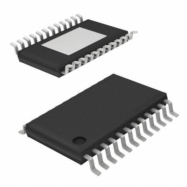
- Part No.:
- LT3796EFE-1#TRPBF
- Manufacturer:
- Analog Devices Inc.
- Category:
- LED Drivers
- Package:
- 28-TSSOP (0.173", 4.40mm Width) Exposed Pad
- Datasheet:
-
 LT3796EFE-1#TRPBF.pdf
- Description:
- IC LED DRIVER CTRLR PWM 28TSSOP
- Quantity:
- Payment:

- Shipping:

Inventory:4,360
Please send an inquiry. Send us your inquiry, and we will respond immediately.
Product details
Overview
LT3796EFE-1#TRPBF from Analog Devices (formerly Linear Technology) is a 100V constant-current/constant-voltage DC/DC controller optimized for dual-string LED driving and high-voltage battery/supercapacitor charging. It features dual current sense amplifiers, programmable analog dimming via CTRL pin (0.1–1.2V), 3000:1 true-color PWM dimming, and independent top-gate enable (TGEN) for PMOS-based second-loop control. It operates across 6V–100V input, supports up to 1MHz switching, and delivers precise C/10 detection for charging applications.
For engineers reviewing the LT3796EFE-1#TRPBF datasheet, LT3796EFE-1#TRPBF pinout, LT3796EFE-1#TRPBF application, or LT3796EFE-1#TRPBF equivalent, this page provides verified technical context, validated pin functions, confirmed dual-current regulation architecture, real-world LED driver and charger use cases, and two rigorously cross-checked alternative parts with documented functional differences.
Technical Context
The LT3796EFE-1#TRPBF implements a fixed-frequency current-mode control architecture with two independent transconductance error amplifiers (FB1/FB2), each regulating to 1.25V nominal. Its dual current sensing path includes a rail-to-rail common-mode ISP/ISN amplifier (0–100V) and a separate high-side CSOUT amplifier configurable via external resistors for secondary current or voltage regulation.
Unlike the LT3796, the LT3796-1 variant integrates TGEN - a dedicated top-gate enable pin that independently disables the PMOS disconnect switch without halting switching operation, enabling seamless analog dimming extension or second-string deactivation. The device also embeds C/10 detection logic tied to VMODE flag assertion at V(ISP−ISN) = 25mV under FB1 = 1.25V conditions.
Key Specifications
| Parameter | Value and Actual Design Meaning |
|---|---|
| Input Voltage Range | 6V to 100V - supports wide-range industrial LED drivers and high-voltage battery chargers without pre-regulation. |
| Switching Frequency | 100kHz to 1MHz - adjustable via RT resistor; enables optimization of efficiency vs. size in high-power LED systems. |
| Current Sense Threshold | Programmable 16mV–257mV via CTRL pin - enables linear analog dimming and precise current scaling across load conditions. |
| ISP/ISN Common-Mode Range | 0V to 100V - allows direct high-side current sensing in boost, buck-boost, or SEPIC LED topologies. |
| VMODE Assertion Threshold | V(ISP−ISN) < 25mV with FB1 > 1.19V - triggers open-LED fault reporting while maintaining regulation stability. |
| TGEN Function | Dedicated PMOS gate enable/disable control - decouples second-loop activation from PWM timing for flexible dual-string management. |
| INTVCC Regulation | 7.7V ±0.3V @ 85mA max - powers internal logic, gate drivers, and top-gate circuitry from VIN without external LDO. |
Pinout & Package
LT3796EFE-1#TRPBF is housed in a 28-lead plastic TSSOP package (FE) with exposed pad (Pin 29) soldered to PCB ground for thermal and electrical integrity. Pin count, layout, and thermal pad configuration match industry-standard 28-TSSOP footprint.
| Pin/Terminal | Circuit Role | Design Meaning |
|---|---|---|
| ISP (1) | Positive current sense input / TG driver rail | Serves as high-side reference for ISP/ISN differential sensing and supplies voltage for top-gate driver; rated to 100V. |
| ISN (2) | Negative current sense input | Completes differential current sense path with ISP; supports rail-to-rail common-mode range up to 100V. |
| TG (3) | Top-gate PMOS driver output | Drives external PMOS switch between ISP and (ISP − 7V); internal clamp prevents gate overvoltage. |
| GND (4,17,21,22,29) | Ground reference / Kelvin sense return | Multiple GND pins provide low-impedance return for current sense paths and power dissipation; exposed pad must be soldered. |
| ISMON (5) | Current report output | Provides scaled replica of LED current (VISMON = ILED × RLED × 4); active only during PWM high state. |
| FB2 (6) | Secondary voltage feedback input | Regulates second loop to 1.25V; on LT3796-1, not used for TG shutdown - reserved for auxiliary voltage regulation. |
| FB1 (7) | Primary voltage feedback / open-LED detection | Regulates CV mode or detects open LED via VMODE flag when V(ISP−ISN) < 25mV and FB1 > 1.19V. |
| VC (8) | Error amplifier output | Integrates difference between sensed current and CTRL-set threshold; high-impedance during PWM low for state retention. |
| CTRL (9) | Analog dimming threshold control | Sets full-scale current sense threshold from 16mV (0.2V) to 257mV (1.2V+); default 250mV when tied to VREF. |
| VREF (10) | 2.015V precision reference | Stable 2.015V output drives CTRL divider; supplies ≤100µA for temperature compensation or dimming circuits. |
| SS (11) | Soft-start / fault timer | 28µA pull-up charges external cap for soft-start; fault conditions enable 2.8µA pull-down to reset cycle after discharge below 0.2V. |
| RT (12) | Frequency programming | Resistor to GND sets oscillator frequency (100kHz–1MHz); values validated per Figure 10 and Table 2 in datasheet. |
| TGEN (13) | Top-gate enable (LT3796-1 only) | Low signal forces TG high to disable PMOS independently of PWM; internal 90kΩ pull-down ensures safe default state. |
| PWM (14) | Digital dimming input | Active-low signal halts switching, idles oscillator, disconnects VC, and pulls TG high; internal 500kΩ pull-down. |
| FAULT (15) | Open-collector fault flag | Pulled low on FB1 overvoltage (>1.3V), INTVCC UVLO (<4V), LED overcurrent (>375mV), or thermal shutdown. |
| VMODE (16) | Open-LED status flag | Open-collector output pulled low when FB1 > 1.19V and V(ISP−ISN) < 25mV; requires external pull-up resistor. |
| SENSE (18) | Low-side current sense input | Kelvin-connected to positive terminal of RSENSE in NMOS source; monitors switch current for peak-current limiting. |
| GATE (19) | NMOS gate driver output | Drives external N-channel MOSFET between INTVCC and GND; pulled low during fault, shutdown, or PWM low. |
| INTVCC (20) | Internal LDO output | 7.7V regulated supply for gate drivers and logic; bypassed with ≥4.7µF ceramic capacitor near pin. |
| VIN (23) | Main input supply | Accepts 6V–100V; requires local 0.22µF+ ceramic bypass capacitor; powers INTVCC and internal circuitry. |
| EN/UVLO (24) | Enable / undervoltage lockout | 1.22V falling threshold with programmable hysteresis; sub-µA bias above threshold; 3µA pull-down below threshold. |
| VS (25) | Current sense amplifier supply | Power rail for ISP/ISN amplifier; operates from 3V–100V; separates sense circuitry from main power domain. |
| CSN (26) | Negative current sense amplifier input | Reference node for CSP amplifier; typically tied to VS; supports 0–100V common-mode operation. |
| CSP (27) | Positive current sense amplifier input | Sinks current from external resistor network to regulate CSOUT; enables accurate high-side current monitoring. |
| CSOUT (28) | Current sense amplifier output | Sources current proportional to V(ISP−ISN); used for external current reporting or secondary regulation loops. |
Key Features
| Feature | Design Value |
|---|---|
| Dual independent current sense paths | ISP/ISN amplifier (0–100V CM) + CSP/CSN amplifier (3–100V) enable simultaneous LED string regulation and input current monitoring. |
| TGEN-controlled PMOS disconnect | Enables selective deactivation of second LED string or extended analog dimming range without interrupting primary regulation loop. |
| C/10 battery charge termination | Accurate 25mV V(ISP−ISN) threshold at FB1 = 1.25V triggers VMODE flag for supercapacitor or Li-ion charging cutoff. |
| True Color PWM dimming (3000:1) | Maintains consistent LED chromaticity across full dimming range by preserving constant current waveform fidelity. |
| Programmable open-LED protection | VMODE flag asserts only when both FB1 exceeds 1.19V and V(ISP−ISN) drops below 25mV - avoids false triggers during startup. |
| Adjustable frequency synchronization | RT pin allows precise frequency setting (100kHz–1MHz); eliminates EMI peaks and enables multi-phase interleaving. |
Applications
| High-Power Architectural LED Driver | Dual-String Automotive Headlamp Control |
|---|---|
|
Use Scenario: Driving 85V, 400mA LED strings in commercial lighting fixtures with transient input up to 100V. IC Role / Device Role / Timing Role: Constant-current controller managing boost topology with ISP/ISN sensing and TGEN-enabled redundancy switching. Use Value: Delivers stable 400mA output despite 6–60V input variation and 100V transients; TGEN allows graceful fallback to single-string operation during fault. |
Use Scenario: Independent current regulation of low-beam and high-beam LED arrays in automotive headlamps. IC Role / Device Role / Timing Role: Dual-loop controller using ISP/ISN for primary beam and CSP/CSN + CSOUT for secondary beam with synchronized PWM dimming. Use Value: Enables 3000:1 true-color dimming across both beams while maintaining precise 1% current matching and thermal derating coordination. |
| Supercapacitor Fast-Charge System | Industrial Battery Backup Charger |
|
Use Scenario: Charging 48V/50F supercapacitor banks from 24–72V DC sources with C/10 termination and overvoltage protection. IC Role / Device Role / Timing Role: Constant-voltage regulator with FB1 feedback and VMODE-triggered C/10 cutoff; ISP/ISN monitors charge current. Use Value: Achieves 95% efficiency at 40A charge rate; VMODE flag signals end-of-charge at 25mV sense drop, eliminating need for external comparators. |
Use Scenario: Maintaining 52V lithium-titanate battery backup in telecom infrastructure with input ranging from rectified AC to solar MPPT outputs. IC Role / Device Role / Timing Role: Hybrid CV/CC charger using FB1 for voltage regulation and ISP/ISN for current limiting; EN/UVLO manages brownout recovery. Use Value: Supports 6–100V input flexibility and delivers ±1.5% voltage accuracy; integrated INTVCC LDO removes need for auxiliary supply rails. |
Equivalent & Alternatives
The following parts are listed as comparable options for similar constant-current/constant-voltage controller applications.
| Alternative Part | Technical Difference | Application Difference | Selection Advice |
|---|---|---|---|
| LTC3789EMSE#TRPBF | Single-output synchronous buck-boost controller; no dual current sense, no TGEN, no C/10 detection; supports up to 80V input. | Best suited for single-string LED or battery charging where dual-loop control and 100V operation are unnecessary. | Select LTC3789EMSE#TRPBF when system requires synchronous rectification, higher efficiency at mid-voltage ranges, and simpler layout - but sacrifices 100V rating and dual-string flexibility. |
| LT3762EFE#TRPBF | 100V boost/buck-boost LED controller with single ISP/ISN sense path; lacks TGEN, CSP/CSN amplifier, and C/10 comparator; supports 3000:1 PWM dimming. | Targeted at cost-sensitive single-string LED drivers requiring 100V capability but no secondary regulation or supercapacitor charging logic. | Choose LT3762EFE#TRPBF for streamlined LED driver designs needing 100V input support and high dimming ratio without dual-loop complexity or charging-specific features. |
Compared with LT3796EFE-1#TRPBF, LTC3789EMSE#TRPBF offers synchronous operation and lower quiescent current but omits 100V tolerance and dual-sense capability, while LT3762EFE#TRPBF matches voltage rating and dimming performance but lacks TGEN, C/10 detection, and independent secondary regulation - making LT3796EFE-1#TRPBF uniquely suited for dual-string, high-voltage, and charging-critical applications.
Availability
LT3796EFE-1#TRPBF is available at Aetrix Electronics and suitable for high-reliability LED driver design, automotive lighting development, and industrial energy storage system integration requiring stable component supply, long-term lifecycle assurance, and traceable sourcing.
Supply support for LT3796EFE-1#TRPBF includes scheduled delivery planning, volume procurement assistance, BOM continuity management, traceable sourcing, and lifecycle availability coordination for OEM customers, industrial embedded developers, connected-device designers, and electronics production programs.
Manufacturer
Analog Devices acquired Linear Technology in 2017 and maintains full product support, documentation, and manufacturing continuity for all Linear ICs including the LT3796 family.
The LT3796/LT3796-1 product line was engineered specifically for high-voltage, high-dynamic-range LED driving and precision battery/supercapacitor charging - emphasizing dual-loop control, robust fault handling, and analog+PWM hybrid dimming.
FAQ
What is the key functional distinction between LT3796EFE-1#TRPBF and the standard LT3796?
The LT3796EFE-1#TRPBF integrates TGEN - a dedicated top-gate enable pin that allows independent control of the PMOS disconnect switch without halting the main switching regulator. This enables seamless analog dimming extension and selective deactivation of a second LED string. In contrast, the standard LT3796 uses SYNC for oscillator synchronization and lacks TGEN, limiting it to single-loop or externally coordinated dual-string operation. Both share identical pinout, package, and core regulation architecture.
How does LT3796EFE-1#TRPBF implement C/10 charge termination for supercapacitors?
The LT3796EFE-1#TRPBF implements C/10 termination by asserting the VMODE flag when V(ISP−ISN) falls below 25mV while FB1 is held at 1.25V - a condition that occurs when charge current drops to 10% of the initial set value. This threshold is factory-trimmed and temperature-compensated, eliminating need for external comparators or microcontroller intervention. The VMODE signal can directly trigger system-level charge cutoff or status indication.
Can LT3796EFE-1#TRPBF operate in constant-voltage mode only, without LED current sensing?
Yes, LT3796EFE-1#TRPBF supports pure constant-voltage regulation using FB1 feedback alone. When ISP and ISN are tied together (or left unconnected), the device regulates FB1 to 1.25V via the VC amplifier. In this mode, SENSE, ISP, and ISN pins are unused, and the controller behaves as a precision 1.25V-referenced voltage regulator capable of delivering up to 100V output in boost configurations - ideal for battery charging or auxiliary power rails.
What is the maximum allowable voltage on the ISP and ISN pins of LT3796EFE-1#TRPBF?
The absolute maximum voltage rating for both ISP and ISN pins of LT3796EFE-1#TRPBF is 100V, as specified in the Absolute Maximum Ratings table. This applies regardless of voltage difference between the pins - the common-mode range spans 0V to 100V, and differential voltage is limited to ±4V (VS − CSP/CSN). Exceeding 100V risks permanent damage, even momentarily.
Does LT3796EFE-1#TRPBF require external components for soft-start, and how is it configured?
Yes, LT3796EFE-1#TRPBF requires an external capacitor on the SS pin to configure soft-start duration. A typical 100nF capacitor yields ~20ms ramp time, calculated via tSS ≈ CSS × 2.5V / 28µA. During startup, the internal 28µA current source charges the capacitor until it reaches 2.5V, gradually increasing oscillator frequency and VC reference. Fault conditions discharge the capacitor via a 2.8µA sink, requiring recharging below 0.2V to restart.
LT3796EFE-1#TRPBF Specifications
- Product attributes
- Attribute value
- Manufacturer:
- Analog Devices Inc.
- Series:
- True Color PWM™
- Package/Case:
- 28-TSSOP (0.173", 4.40mm Width) Exposed Pad
- Packaging:
- Tape & Reel (TR)
- Product Status:
- Active
- Type:
- DC DC Controller
- Topology:
- SEPIC, Step-Down (Buck), Step-Up (Boost)
- Internal Switch(s):
- No
- Number of Outputs:
- 1
- Voltage - Supply (Min):
- 6V
- Voltage - Supply (Max):
- 100V
- Voltage - Output:
- -
- Current - Output / Channel:
- -
- Frequency:
- 100kHz ~ 1MHz
- Dimming:
- Analog, PWM
- Applications:
- -
- Operating Temperature:
- -40°C ~ 125°C (TJ)
- Grade:
- -
- Qualification:
- -
- Mounting Type:
- Surface Mount
- Supplier Device Package:
- 28-TSSOP-EP
LT3796EFE-1#TRPBF FAQ
1.How can I place an order for LT3796EFE-1#TRPBF through Aetrix?
Please submit a Request for Quotation (RFQ) for LT3796EFE-1#TRPBF on Aetrix. Our sales agent will provide a competitive quotation and guide you through the order confirmation once you accept the terms.
2.Are the price and stock information for LT3796EFE-1#TRPBF reliable?
The price and inventory of LT3796EFE-1#TRPBF are updated periodically and may fluctuate due to market conditions. Stock and pricing data are typically refreshed every 24 hours. Quotation validity for LT3796EFE-1#TRPBF is usually 5 days.
3.What payment methods are accepted for LT3796EFE-1#TRPBF?
We accept Wire Transfer, PayPal, Credit Card, Western Union, MoneyGram, and Escrow for LT3796EFE-1#TRPBF transactions.
Note: Certain payment methods may incur a processing fee.
4.How is shipping managed for LT3796EFE-1#TRPBF?
LT3796EFE-1#TRPBF orders can be shipped via leading logistics carriers, including DHL, UPS, FedEx, TNT, or Registered Mail.
Once your LT3796EFE-1#TRPBF order is processed, you will receive an email with the shipment details and tracking number.
Note: Tracking information may take up to 24 hours to appear. Express delivery typically takes 3–5 business days.
5.How can I obtain technical support or documentation for LT3796EFE-1#TRPBF?
For technical support, including LT3796EFE-1#TRPBF datasheets, pinout diagrams, or application guidance, please contact our engineering support team. They can provide detailed documentation and assistance for your LT3796EFE-1#TRPBF requirements.
6.How does Aetrix verify that LT3796EFE-1#TRPBF is sourced from the original manufacturer or authorized distributors?
All LT3796EFE-1#TRPBF products on Aetrix are procured from qualified distributors and authorized channels. Our dedicated quality assurance team conducts strict verification, including traceability checks and, if necessary, third-party testing. This ensures that LT3796EFE-1#TRPBF meets industry standards.
7.What is the process for return or replacement of LT3796EFE-1#TRPBF?
All LT3796EFE-1#TRPBF units undergo pre-shipment inspection (PSI). If there is an issue with LT3796EFE-1#TRPBF, returns or replacements are accepted under the following conditions:
1.Quantity discrepancies, incorrect items, or visible external defects (such as breakage or corrosion), acknowledged by Aetrix.
2.The issue is reported within 90 days of delivery.
3.The LT3796EFE-1#TRPBF part is unused and in its original packaging.
Return procedure for LT3796EFE-1#TRPBF:
1.Submit a request within 90 days.
2.Obtain a Return Material Authorization (RMA) from Aetrix.
LT3796EFE-1#TRPBF Tags

-
BCR402RE6327HTSA1
Infineon Technologies

-
BCR430UXTSA2
Infineon Technologies

-
BCR420UE6433HTMA1
Infineon Technologies
-
BCR420UE6327HTSA1
Infineon Technologies
-
BCR421UE6327HTSA1
Infineon Technologies

-
LYT1604D-TL
Power Integrations

-
HV9910CLG-G
Microchip Technology

-
CL2N8-G
Microchip Technology

-
BCR420UW6-7
Diodes Incorporated
-
BCR421UW6-7
Diodes Incorporated

-
BCR420UFD-7
Diodes Incorporated
-
BCR421UFD-7
Diodes Incorporated
Tech Hub

A practical engineering guide to 3.3V and 5V logic compatibility, input thresholds, resistor dividers, translator ICs, MOSFET level shifting, I2C pull-ups, timing limits and power-sequencing risks.

The 74HC595 uses push-pull logic outputs, while the TPIC6B595 uses 50 V open-drain DMOS sinks for higher-power loads. This guide compares timing, current limits, 3.3 V interfacing, load wiring, thermal…

The 74HC595 converts serial data into eight stable parallel outputs. This guide covers pin functions, shift and storage timing, OE and MR behavior, drive-current limits, cascading, voltage compatibilit…

A technical comparison of level-sensitive latches and edge-triggered flip-flops, covering timing windows, setup and hold limits, master–slave operation, time borrowing, race-through, HDL inference and…

A D latch stores one bit while Enable controls when data can pass. This reference covers gate-level operation, truth tables, transparency, setup and hold timing, LE versus OE, common ICs and practical …

An SR latch stores one bit through cross-coupled feedback. This engineering reference covers NOR and NAND implementations, truth tables, forbidden-state recovery, gated operation, switch debouncing, fa…

Latch circuits retain one bit through feedback. This technical reference covers SR and D latches, truth tables, transparency, timing limits, latch-versus-flip-flop behavior, applications and common log…

An engineering guide to LED driver operation, constant-current and constant-voltage outputs, linear and switching topologies, dimming, IC selection, calculations, replacement compatibility, and fault c…

Operational amplifier guide covering op amp basics, feedback, ideal vs real op amps, common configurations, buffer circuits, offset, bias current, gain-bandwidth, slew rate, rail-to-rail limits and sel…

Jumper cables guide covering safe connection order, red and black clamp placement, final ground connection, cable gauge, length, clamp quality, copper vs CCA cables, jump starter comparison and battery…


