
 My Inquiry
 My Account


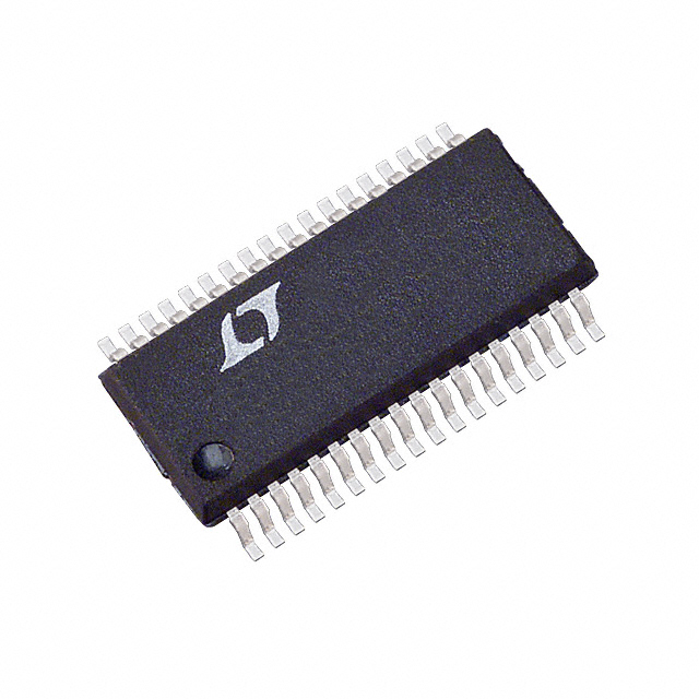
Analog Devices Inc. LTC1411IG#PBF
- Part No.:
- LTC1411IG#PBF
- Manufacturer:
- Analog Devices Inc.
- Category:
- Analog to Digital Converters (ADC)
- Package:
- 36-SSOP (0.209", 5.30mm Width)
- Datasheet:
-
 LTC1411IG#PBF.pdf
- Description:
- IC ADC 14BIT SAR 36SSOP
- Quantity:
- Payment:

- Shipping:

Inventory:2,369
Please send an inquiry. Send us your inquiry, and we will respond immediately.
Product details
Overview
LTC1411IG#PBF from Analog Devices (formerly Linear Technology) is a 14-bit, 2.5 Msps successive-approximation ADC with true differential inputs, internal 2.5V reference, programmable ±1.8V/±1.27V/±0.9V/±0.64V input ranges, and single 5V supply operation. It delivers ±2 LSB INL, 80 dB S/(N+D) at 100 kHz, and no pipeline delay - enabling high-fidelity signal acquisition in telecom and DSP systems.
For engineers reviewing the LTC1411IG#PBF datasheet, LTC1411IG#PBF pinout, LTC1411IG#PBF application, or LTC1411IG#PBF equivalent, key selection factors include its 36-pin SSOP package, Nap/Sleep shutdown modes (2 mA / 1 µA), out-of-range detection via OTR/D13, and compatibility with FIFOs, DSPs, and microprocessors via simple CONVST/BUSY interface.
Technical Context
The LTC1411IG#PBF employs a capacitor-based SAR architecture with integrated sample-and-hold, factory-trimmed internal clock (260 ns conversion time), and differential input stage rejecting common-mode noise up to 62 dB. Its analog front-end supports both differential and single-ended configurations with AIN– serving as bipolar zero reference point.
Control logic responds to active-low CONVST to initiate conversion; BUSY goes low during conversion and rises ~250–350 ns later, with valid 2's complement data appearing 7 ns after BUSY↑. Programmable gain is set by PGA0/PGA1 pins, altering REFCOM2 voltage (4.05 V down to 1.45 V) to scale full-scale span without external components.
Key Specifications
| Parameter | Value and Actual Design Meaning |
|---|---|
| Resolution | 14-bit with no missing codes over temperature - guarantees monotonicity and full dynamic range utilization. |
| Sampling Rate | 2.5 Msps maximum - supports real-time digitization of signals up to 1.25 MHz Nyquist bandwidth. |
| S/(N + D) | 80 dB at 100 kHz input - enables >12.7 effective bits for precision measurement applications. |
| INL | ±2 LSB max - ensures accurate amplitude representation across full code range, critical for calibration-sensitive systems. |
| Power Dissipation | 195 mW typical at 5 V - balances speed and thermal load in space-constrained industrial or telecom modules. |
| Shutdown Current | 1 µA in Sleep mode - allows ultra-low-power standby in battery-backed data loggers or portable instrumentation. |
| Input Range | Four software-selectable spans (±1.8 V to ±0.64 V) - simplifies sensor interfacing without external gain stages. |
Pinout & Package
The LTC1411IG#PBF is housed in a 36-pin plastic SSOP (G package) with exposed pad thermal enhancement. Pin assignments are validated per Linear Technology LTC1411 datasheet Rev. F and match the top-view pinout diagram on page 2.
| Pin/Terminal | Circuit Role | Design Meaning |
|---|---|---|
| AIN+, AIN– (1, 2) | Differential analog inputs | Accept true differential or single-ended signals; common-mode range 0 V to VDD supports rail-to-rail sensing. |
| REFOUT (3) | 2.5 V internal reference output | Provides stable bipolar zero when tied to AIN–; requires 22 µF tantalum bypass if used directly. |
| REFIN (4) | External reference input | Allows higher-precision 2.5 V sources (e.g., LT1019A-2.5) to override internal reference for <5 ppm/°C drift. |
| REFCOM1, REFCOM2 (5, 6) | Noise reduction & reference compensation | Require 10 µF tantalum + 0.1 µF ceramic bypassing to stabilize PGA gain-setting voltage and suppress reference noise. |
| AGND1–3 (7–9) | Analog ground returns | Must be connected to single-point analog ground plane - separates reference, comparator, and core analog circuitry. |
| AVP (10) | Analog power supply | 5 V supply for analog section; requires 10 µF tantalum bypass to AGND1 to minimize switching noise coupling. |
| AVM (11) | Analog/digital substrate tie | Connect directly to AGND to prevent latch-up and reduce substrate noise injection into analog core. |
| D13–D0 (12–25) | Parallel digital outputs | 14-bit 2's complement data bus (D13 = MSB); outputs drive standard CMOS loads with VOH ≥ 4.0 V @ –200 µA. |
| OTR (26) | Out-of-range indicator | Active-high flag used with D13 to distinguish overrange (D13=0, OTR=1) from underrange (D13=1, OTR=1). |
| BUSY (27) | Conversion status | Active-low open-drain output signaling ongoing conversion; timing-critical for synchronous data capture. |
| OGND, OVDD (28, 29) | Digital output ground/supply | Isolated 3 V or 5 V domain for output drivers - prevents digital noise from corrupting analog measurements. |
| DVP (30) | Digital power supply | 5 V supply for internal logic; bypassed to OGND with 10 µF tantalum to decouple CONVST/NAP/SLP switching transients. |
| DGND (31) | Digital ground | Return path for CONVST, NAP, SLP, PGA0/PGA1 - must tie to OGND but remain isolated from AGND. |
| CONVST (32) | Conversion start trigger | Falling-edge sensitive control input; minimum pulse width 20 ns - compatible with FPGA or microcontroller GPIO. |
| PGA0, PGA1 (33, 34) | Programmable gain select | Two-pin binary encoding selects one of four input spans; logic levels must be stable ≥700 ms before conversion if changing range. |
| NAP (35) | Nap mode enable | Pull-down enabled; driving low reduces current to 2 mA while preserving internal reference for external use. |
| SLP (36) | Sleep mode enable | Pull-down enabled; driving low cuts current to <1 µA - wake-up requires 210 ms for full reference stabilization. |
Key Features
| Feature | Design Value |
|---|---|
| True differential input architecture | Rejects common-mode noise up to 62 dB - improves SNR in noisy industrial environments without external instrumentation amps. |
| Internal 2.5 V bandgap reference | Factory trimmed to ±20 mV (±0.8%) and tempco ≤±15 ppm/°C - eliminates need for external reference in cost-sensitive designs. |
| No pipeline delay | Delivers first valid sample within one conversion cycle - essential for closed-loop control and real-time feedback systems. |
| Out-of-range detection with OTR/D13 | Enables automatic signal clipping or gain adjustment in software without external comparators or ADC monitoring logic. |
| Independent analog/digital supply domains | Separate AVP, DVP, OVDD rails with dedicated ground pins - minimizes crosstalk between sampling and data output stages. |
Applications
| Telecommunications Baseband Processing | Digital Signal Processing Front-End |
|---|---|
Use Scenario: Digitizing IF signals in wireless infrastructure equipment operating at 100–500 kHz with strict linearity requirements. IC Role / Device Role / Timing Role: High-speed ADC capturing baseband I/Q channels with minimal harmonic distortion and no latency-induced phase error. Use Value: 90 dB THD at 100 kHz and 80 dB S/(N+D) ensure clean spectral reconstruction for OFDM symbol decoding and adjacent-channel rejection. | Use Scenario: Feeding real-time sensor data into TI C6000 or Analog Devices SHARC DSPs for vibration analysis or audio processing. IC Role / Device Role / Timing Role: Parallel-output ADC synchronized to DSP external memory interface using CONVST/BUSY handshake. Use Value: No pipeline delay and 2.5 Msps throughput allow deterministic sample-to-process latency critical for adaptive filtering algorithms. |
| Multiplexed Data Acquisition Systems | High-Speed Imaging Sensor Interface |
Use Scenario: Scanning multiple thermocouple or strain gauge channels via analog multiplexer in automated test equipment. IC Role / Device Role / Timing Role: ADC with programmable input ranges adapting to varying sensor output spans without hardware reconfiguration. Use Value: Four PGA-selectable spans (±1.8 V to ±0.64 V) eliminate external gain-switching circuitry and reduce BOM count per channel. | Use Scenario: Capturing line-scan CCD or CMOS image sensor outputs requiring precise DC offset control and wide dynamic range. IC Role / Device Role / Timing Role: Bipolar 2's complement ADC with AIN– referenced to REFOUT providing consistent black-level alignment across frames. Use Value: ±2 LSB INL and 14-bit no-missing-code performance preserve fine intensity gradations in medical or scientific imaging. |
Equivalent & Alternatives
The following parts are listed as comparable options for similar high-speed precision ADC applications.
| Alternative Part | Technical Difference | Application Difference | Selection Advice |
|---|---|---|---|
| AD9240ASTZ-25 | 14-bit, 25 MSPS pipelined ADC; requires external reference and clock; higher power (1.2 W); no Nap/Sleep modes. | Better suited for undersampling RF applications above Nyquist; not drop-in due to different timing model and pinout. | Select when >2.5 MSPS throughput or RF input frequencies >10 MHz are required; avoid if low-power or simple interface is prioritized. |
| MAX1186ETL+ | 14-bit, 2.5 MSPS SAR ADC; 20-pin TQFN; internal reference; only two input ranges (±2.048 V, ±1.024 V); no OTR pin. | Compact footprint ideal for portable instruments; lacks out-of-range detection and flexible PGA scaling. | Choose for space-constrained designs where simplified range selection suffices and OTR functionality is unnecessary. |
Compared with AD9240ASTZ-25 and MAX1186ETL+, the LTC1411IG#PBF uniquely combines 2.5 Msps speed, four programmable input spans, integrated reference, and dual shutdown modes in a single 36-pin SSOP package - making it optimal for medium-speed, feature-rich embedded data acquisition where power, flexibility, and ease of interface are balanced.
Availability
LTC1411IG#PBF is available at Aetrix Electronics and suitable for telecommunications baseband processing, digital signal processing front-ends, and multiplexed data acquisition systems requiring stable component supply across extended temperature ranges (–40°C to +85°C).
Supply support for LTC1411IG#PBF includes scheduled delivery planning, volume procurement assistance, BOM continuity management, traceable sourcing, and lifecycle availability coordination for OEM customers, industrial embedded developers, connected-device designers, and electronics production programs.
Manufacturer
Analog Devices, Inc. (ADI) is a global leader in high-performance analog, mixed-signal, and digital signal processing technologies, acquired Linear Technology in 2017 to expand precision converter and power management portfolios.
The LTC1411IG#PBF belongs to Linear Technology's legacy high-speed precision ADC family, designed specifically for applications demanding excellent AC performance, low power, and seamless microprocessor/DSP interfacing in industrial, medical, and communications equipment.
FAQ
What is the operating temperature range for the LTC1411IG#PBF?
The LTC1411IG#PBF is specified for operation from –40°C to +85°C (Industrial grade). This is confirmed in the "Order Information" table on page 2 of the datasheet, where "LTC1411IG" denotes the Industrial temperature version. The "C" grade (0°C to 70°C) is distinct and not applicable to this part number.
Does the LTC1411IG#PBF require an external clock source?
No, the LTC1411IG#PBF does not require an external clock. It contains a factory-trimmed internal clock that guarantees a 2.5 Msps sampling rate with typical conversion time of 260 ns and acquisition time of 100 ns. External clocking is not supported - timing is fully controlled by the CONVST signal.
How does the out-of-range (OTR) function work on the LTC1411IG#PBF?
The LTC1411IG#PBF uses OTR in conjunction with D13 (MSB) to indicate overrange or underrange conditions. Per the truth table in Figure 8 and datasheet Table 2: OTR = 1 and D13 = 0 indicates overrange; OTR = 1 and D13 = 1 indicates underrange. This dual-signal scheme avoids ambiguity inherent in single-pin overflow flags.
Can the LTC1411IG#PBF operate with a 3.3 V digital supply?
Yes - the LTC1411IG#PBF supports OVDD = 3 V or 5 V for its digital output drivers (pins D13–D0, OTR, BUSY), as explicitly stated in the "Digital Inputs and Outputs" section (page 3). However, AVP and DVP must remain at 5 V, and the analog input common-mode range remains 0 V to VDD (5 V), so signal conditioning must respect this constraint.
What is the recommended bypassing for the REFCOM2 pin on the LTC1411IG#PBF?
The datasheet specifies a 10 µF tantalum capacitor in parallel with a 0.1 µF ceramic capacitor from REFCOM2 (pin 6) to AGND1. This dual-capacitor configuration stabilizes the PGA gain-setting voltage during range changes and suppresses high-frequency noise that would otherwise degrade reference accuracy and THD performance.
LTC1411IG#PBF Specifications
- Product attributes
- Attribute value
- Manufacturer:
- Analog Devices Inc.
- Series:
- -
- Package/Case:
- 36-SSOP (0.209", 5.30mm Width)
- Packaging:
- Tube
- Product Status:
- Active
- Number of Bits:
- 14
- Sampling Rate (Per Second):
- 2.5M
- Number of Inputs:
- 1
- Input Type:
- Differential, Single Ended
- Data Interface:
- Parallel
- Configuration:
- S/H-ADC
- Ratio - S/H:ADC:
- 1:1
- Number of A/D Converters:
- 1
- Architecture:
- SAR
- Reference Type:
- External, Internal
- Voltage - Supply, Analog:
- 5V
- Voltage - Supply, Digital:
- 5V
- Features:
- -
- Operating Temperature:
- -40°C ~ 85°C
- Supplier Device Package:
- 36-SSOP
- Mounting Type:
- Surface Mount
- Grade:
- -
- Qualification:
- -
LTC1411IG#PBF FAQ
1.How can I place an order for LTC1411IG#PBF through Aetrix?
Please submit a Request for Quotation (RFQ) for LTC1411IG#PBF on Aetrix. Our sales agent will provide a competitive quotation and guide you through the order confirmation once you accept the terms.
2.Are the price and stock information for LTC1411IG#PBF reliable?
The price and inventory of LTC1411IG#PBF are updated periodically and may fluctuate due to market conditions. Stock and pricing data are typically refreshed every 24 hours. Quotation validity for LTC1411IG#PBF is usually 5 days.
3.What payment methods are accepted for LTC1411IG#PBF?
We accept Wire Transfer, PayPal, Credit Card, Western Union, MoneyGram, and Escrow for LTC1411IG#PBF transactions.
Note: Certain payment methods may incur a processing fee.
4.How is shipping managed for LTC1411IG#PBF?
LTC1411IG#PBF orders can be shipped via leading logistics carriers, including DHL, UPS, FedEx, TNT, or Registered Mail.
Once your LTC1411IG#PBF order is processed, you will receive an email with the shipment details and tracking number.
Note: Tracking information may take up to 24 hours to appear. Express delivery typically takes 3–5 business days.
5.How can I obtain technical support or documentation for LTC1411IG#PBF?
For technical support, including LTC1411IG#PBF datasheets, pinout diagrams, or application guidance, please contact our engineering support team. They can provide detailed documentation and assistance for your LTC1411IG#PBF requirements.
6.How does Aetrix verify that LTC1411IG#PBF is sourced from the original manufacturer or authorized distributors?
All LTC1411IG#PBF products on Aetrix are procured from qualified distributors and authorized channels. Our dedicated quality assurance team conducts strict verification, including traceability checks and, if necessary, third-party testing. This ensures that LTC1411IG#PBF meets industry standards.
7.What is the process for return or replacement of LTC1411IG#PBF?
All LTC1411IG#PBF units undergo pre-shipment inspection (PSI). If there is an issue with LTC1411IG#PBF, returns or replacements are accepted under the following conditions:
1.Quantity discrepancies, incorrect items, or visible external defects (such as breakage or corrosion), acknowledged by Aetrix.
2.The issue is reported within 90 days of delivery.
3.The LTC1411IG#PBF part is unused and in its original packaging.
Return procedure for LTC1411IG#PBF:
1.Submit a request within 90 days.
2.Obtain a Return Material Authorization (RMA) from Aetrix.
LTC1411IG#PBF Tags
-
ADC081C021CIMKX/NOPB
Texas Instruments

-
MCP3021A5T-E/OT
Microchip Technology
-
TLA2024IRUGR
Texas Instruments
-
MCP3221A5T-E/OT
Microchip Technology
-
MCP3221A5T-I/OT
Microchip Technology
-
MCP3221A4T-E/OT
Microchip Technology
-
MCP3221A6T-E/OT
Microchip Technology
-
MCP3221A0T-E/OT
Microchip Technology
-
MCP3221A1T-E/OT
Microchip Technology

-
ADC121S021CIMFX/NOPB
Texas Instruments

-
MCP3001-I/MS
Microchip Technology

-
MCP3001-I/SN
Microchip Technology
Tech Hub

A practical engineering guide to 3.3V and 5V logic compatibility, input thresholds, resistor dividers, translator ICs, MOSFET level shifting, I2C pull-ups, timing limits and power-sequencing risks.

The 74HC595 uses push-pull logic outputs, while the TPIC6B595 uses 50 V open-drain DMOS sinks for higher-power loads. This guide compares timing, current limits, 3.3 V interfacing, load wiring, thermal…

The 74HC595 converts serial data into eight stable parallel outputs. This guide covers pin functions, shift and storage timing, OE and MR behavior, drive-current limits, cascading, voltage compatibilit…

A technical comparison of level-sensitive latches and edge-triggered flip-flops, covering timing windows, setup and hold limits, master–slave operation, time borrowing, race-through, HDL inference and…

A D latch stores one bit while Enable controls when data can pass. This reference covers gate-level operation, truth tables, transparency, setup and hold timing, LE versus OE, common ICs and practical …

An SR latch stores one bit through cross-coupled feedback. This engineering reference covers NOR and NAND implementations, truth tables, forbidden-state recovery, gated operation, switch debouncing, fa…

Latch circuits retain one bit through feedback. This technical reference covers SR and D latches, truth tables, transparency, timing limits, latch-versus-flip-flop behavior, applications and common log…

An engineering guide to LED driver operation, constant-current and constant-voltage outputs, linear and switching topologies, dimming, IC selection, calculations, replacement compatibility, and fault c…

Operational amplifier guide covering op amp basics, feedback, ideal vs real op amps, common configurations, buffer circuits, offset, bias current, gain-bandwidth, slew rate, rail-to-rail limits and sel…

Jumper cables guide covering safe connection order, red and black clamp placement, final ground connection, cable gauge, length, clamp quality, copper vs CCA cables, jump starter comparison and battery…


