
 My Inquiry
 My Account


Analog Devices Inc. LTC2123CUK#PBF
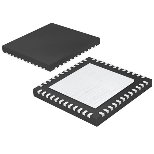
- Part No.:
- LTC2123CUK#PBF
- Manufacturer:
- Analog Devices Inc.
- Category:
- Analog to Digital Converters (ADC)
- Package:
- 48-WFQFN Exposed Pad
- Datasheet:
-
 LTC2123CUK#PBF.pdf
- Description:
- IC ADC 14BIT PIPELINED 48QFN
- Quantity:
- Payment:

- Shipping:

Inventory:2,170
Please send an inquiry. Send us your inquiry, and we will respond immediately.
Product details
Overview
LTC2123CUK#PBF from Analog Devices (formerly Linear Technology) is a dual-channel, 14-bit, 250Msps analog-to-digital converter with JESD204B serial interface, designed for high-frequency signal digitization in communications infrastructure. It delivers 70dBFS SNR, 90dBFS SFDR, and 1.25GHz full-power analog input bandwidth, operating from a single 1.8V supply with 864mW total power consumption.
For engineers reviewing the LTC2123CUK#PBF datasheet, LTC2123CUK#PBF pinout, LTC2123CUK#PBF application, or LTC2123CUK#PBF equivalent, key selection considerations include JESD204B lane configuration (2- or 4-lane), deterministic latency support (Subclass 1/2), clock divide-by-two capability, and CML output drive compliance with 5Gbps per lane.
Technical Context
The LTC2123CUK#PBF integrates two simultaneous-sampling ADC cores with independent analog front-ends, each supporting differential 1.5VP-P input range and programmable internal/external reference via SENSE pin. Its on-chip PLL and configurable clock divider enable operation with either 250MHz or 500MHz DEVCLK inputs.
JESD204B serializer supports both 2-lane (1 lane per channel, 5Gbps/lane) and 4-lane (2 lanes per channel, 2.5Gbps/lane) modes, with deterministic latency established via SYSREF (Subclass 1) or SYNC~ (Subclass 2) synchronization signals and alignment sequence detection.
Key Specifications
| Parameter | Value and Actual Design Meaning |
|---|---|
| Resolution | 14-bit with no missing codes - guarantees monotonic transfer function for precision measurement applications. |
| Sampling Rate | 250Msps - enables Nyquist-limited digitization of signals up to 125MHz or wideband undersampling of RF carriers. |
| SNR / SFDR | 70dBFS / 90dBFS at 70MHz input - provides high dynamic range for cellular base station receiver IF sampling. |
| Analog Bandwidth | 1.25GHz full-power - supports direct RF sampling of L-band and S-band signals without external filtering. |
| Power Consumption | 864mW at 250Msps - balances performance and thermal management in dense FPGA-ADC interfacing layouts. |
| JESD204B Speed | 5Gbps per lane - reduces PCB routing complexity versus parallel LVDS interfaces while maintaining deterministic latency. |
| Supply Voltage | 1.8V analog (VDD), 1.2–1.9V output (OVDD) - simplifies power delivery architecture with single low-noise regulator. |
Pinout & Package
48-lead (7mm × 7mm) plastic QFN package with exposed thermal pad (Pin 49 = GND). Requires soldering of exposed pad to PCB ground plane for thermal and electrical integrity.
| Pin/Terminal | Circuit Role | Design Meaning |
|---|---|---|
| VDD (Pins 1,12,13,23,24,37,38,48) | Analog supply input | 1.8V power rail requiring local 0.1µF ceramic bypass; multiple pins reduce IR drop and inductance. |
| AINA+/AINA–, AINB+/AINB– (Pins 3,4,9,10) | Differential analog inputs | High-Z, 1.5VP-P full-scale range; matched pair routing critical for CMRR >75dB. |
| DEVCLK+/DEVCLK– (Pins 15,16) | Differential sampling clock input | Accepts sine wave, PECL, or LVDS; supports optional divide-by-two for 500MHz clock input at 250Msps. |
| CMLOUT_A0+/A0–, A1+/A1–, B0+/B0–, B1+/B1– (Pins 31–34,27–30) | JESD204B CML serial outputs | 50Ω single-ended or 100Ω differential termination required; 5Gbps capable with <0.35UI jitter. |
| SYSREF+/SYSREF– (Pins 18,19), SYNC~+/SYNC~– (Pins 21,22) | JESD204B synchronization inputs | Enable deterministic latency: SYSREF for Subclass 1, SYNC~ for Subclass 2; timing margins ≤0.6ns. |
Key Features
| Feature | Design Value |
|---|---|
| Optional clock divide-by-two | Enables use of 500MHz clock source while maintaining 250Msps sampling rate, relaxing clock generation requirements. |
| Programmable reference mode | SENSE pin selects internal 1.25V reference (±0.75V input) or external 1.2–1.3V reference (±0.6×VSENSE input). |
| Low-power sleep and nap modes | Reduces power to 2mW (sleep) or 468mW (nap), enabling rapid wake-up for burst-mode signal acquisition. |
| Integrated VCM and VREF outputs | VCM = 0.435×VDD (±18mV) and VREF = 1.25V (±25mV) provide precise biasing without external components. |
| 864mW total power at 250Msps | Optimized for FPGA-based systems where thermal density and power delivery efficiency are critical constraints. |
Applications
| Cellular Base Stations | Software Defined Radios |
|---|---|
Use Scenario: Digitizing multi-carrier LTE or 5G NR IF signals in macrocell remote radio heads. IC Role / Device Role / Timing Role: Dual-channel ADC capturing I/Q data streams with deterministic latency for MIMO beamforming. Use Value: 90dBFS SFDR prevents adjacent channel interference; JESD204B reduces FPGA pin count by >70% vs. parallel LVDS. | Use Scenario: Reconfigurable wideband receiver front-end in military comms or spectrum monitoring equipment. IC Role / Device Role / Timing Role: High-bandwidth ADC enabling real-time FFT analysis across 125MHz instantaneous bandwidth. Use Value: 1.25GHz input bandwidth allows direct sampling of UHF/VHF bands; low aperture jitter (0.15ps RMS) preserves EVM. |
| Medical Imaging | Test and Measurement Instrumentation |
Use Scenario: Ultrasound beamformer digitizing echo return signals from phased-array transducers. IC Role / Device Role / Timing Role: Simultaneous sampling ADC providing time-aligned I/Q data for digital beam steering. Use Value: 70dBFS SNR ensures accurate tissue contrast resolution; crosstalk <–90dB prevents channel bleed in multi-element arrays. | Use Scenario: High-speed oscilloscope or vector signal analyzer digitizing RF modulated waveforms. IC Role / Device Role / Timing Role: Precision ADC core delivering calibrated amplitude and phase accuracy for signal integrity validation. Use Value: Integral linearity ±0.85LSB and differential linearity ±0.25LSB minimize harmonic distortion in spectral analysis. |
Equivalent & Alternatives
The following parts are listed as comparable options for similar high-speed ADC applications.
| Alternative Part | Technical Difference | Application Difference | Selection Advice |
|---|---|---|---|
| AD9680BCPZ-500 | 14-bit, 500Msps, JESD204B, but requires 3.3V OVDD and has higher 1.6W power draw. | Higher sampling rate suits wider instantaneous bandwidth needs; less suitable for thermally constrained 1U chassis. | Select when >250Msps bandwidth is required and power budget allows +850mW overhead. |
| LTC2262IUK#PBF | 12-bit, 105Msps, parallel LVDS output, no JESD204B, lower 350mW power, 48-QFN same footprint. | Lacks deterministic latency and high-speed serial interface; suited for cost-sensitive, non-synchronized systems. | Select when JESD204B is unnecessary and lower resolution/speed meets system SNR and bandwidth targets. |
Compared with AD9680BCPZ-500 and LTC2262IUK#PBF, the LTC2123CUK#PBF uniquely balances 250Msps sampling, 70dBFS SNR, and 5Gbps JESD204B in a thermally efficient 1.8V package-making it optimal for FPGA-based communications systems requiring deterministic latency without overspec'ed speed or power.
Availability
LTC2123CUK#PBF is available at Aetrix Electronics and suitable for cellular base stations, software defined radios, and test instrumentation requiring stable component supply, long-term obsolescence planning, and traceable sourcing for production ramp.
Supply support for LTC2123CUK#PBF includes scheduled delivery planning, volume procurement assistance, BOM continuity management, traceable sourcing, and lifecycle availability coordination for OEM customers, industrial embedded developers, connected-device designers, and electronics production programs.
Manufacturer
Analog Devices, Inc. (acquired Linear Technology in 2017) is a global leader in high-performance analog, mixed-signal, and DSP solutions for precision and high-speed applications.
The LTC2123CUK#PBF belongs to Linear's high-speed ADC product line, engineered specifically for demanding communications infrastructure where JESD204B interoperability, low jitter, and wide analog bandwidth are mandatory.
FAQ
What is the operating temperature range for the LTC2123CUK#PBF?
The LTC2123CUK#PBF is rated for 0°C to 70°C ambient operation (Commercial grade). This is confirmed by the "C" suffix in the part number and the order information table specifying "0°C to 70°C" for LTC2123CUK#PBF. The device uses the same 48-lead QFN package as the industrial-grade LTC2123IUK#PBF but is characterized and tested only over the commercial temperature range.
Does the LTC2123CUK#PBF support JESD204B Subclass 2 deterministic latency?
Yes, the LTC2123CUK#PBF supports JESD204B Subclass 2. The datasheet explicitly states that a low-to-high transition of SYNC~ sampled on the rising edge of DEVCLK initializes the internal dividers and sets up deterministic latency in Subclass 2. Latency values (e.g., LATSC4 = 20tS, LATSL4 = 12tS) are provided for both 2-lane and 4-lane modes under Subclass 2 conditions.
What is the maximum analog input frequency supported by the LTC2123CUK#PBF?
The LTC2123CUK#PBF has a 1.25GHz full-power analog input bandwidth (BW–3dB), meaning it maintains specified dynamic performance (e.g., SNR, SFDR) up to 1.25GHz. This enables undersampling of RF carriers in the L-band (1–2GHz) and S-band (2–4GHz), as demonstrated in typical performance plots showing usable response at 383.1MHz and 907.1MHz inputs.
How is the reference voltage configured on the LTC2123CUK#PBF?
The LTC2123CUK#PBF reference is configured via the SENSE pin (Pin 5). Connecting SENSE to VDD selects the internal 1.25V reference and ±0.75V input range. Applying an external voltage between 1.2V and 1.3V to SENSE selects external reference mode with ±0.6×VSENSE input range. This is documented in the PIN FUNCTIONS section and confirmed by the SENSE input leakage and voltage specifications.
What are the power supply requirements for the LTC2123CUK#PBF OVDD pins?
The LTC2123CUK#PBF requires OVDD (Pins 25,26,35,36) to be supplied with 1.2V to 1.9V. This supply powers the CML output drivers. The datasheet specifies OVDD = 1.2V to 1.9V (min/max) and recommends bypassing each OVDD pair to ground with a 0.1µF ceramic capacitor. Output current per lane is 11–13.8mA at 12mA nominal drive, directly impacting termination voltage selection.
LTC2123CUK#PBF Specifications
- Product attributes
- Attribute value
- Manufacturer:
- Analog Devices Inc.
- Series:
- -
- Package/Case:
- 48-WFQFN Exposed Pad
- Packaging:
- Tube
- Product Status:
- Active
- Number of Bits:
- 14
- Sampling Rate (Per Second):
- 250M
- Number of Inputs:
- 2
- Input Type:
- Differential
- Data Interface:
- JESD204B
- Configuration:
- S/H-ADC
- Ratio - S/H:ADC:
- 1:1
- Number of A/D Converters:
- 2
- Architecture:
- Pipelined
- Reference Type:
- External, Internal
- Voltage - Supply, Analog:
- 1.7V ~ 1.9V
- Voltage - Supply, Digital:
- 1.7V ~ 1.9V
- Features:
- Simultaneous Sampling
- Operating Temperature:
- 0°C ~ 70°C
- Supplier Device Package:
- 48-QFN (7x7)
- Mounting Type:
- Surface Mount
- Grade:
- -
- Qualification:
- -
LTC2123CUK#PBF FAQ
1.How can I place an order for LTC2123CUK#PBF through Aetrix?
Please submit a Request for Quotation (RFQ) for LTC2123CUK#PBF on Aetrix. Our sales agent will provide a competitive quotation and guide you through the order confirmation once you accept the terms.
2.Are the price and stock information for LTC2123CUK#PBF reliable?
The price and inventory of LTC2123CUK#PBF are updated periodically and may fluctuate due to market conditions. Stock and pricing data are typically refreshed every 24 hours. Quotation validity for LTC2123CUK#PBF is usually 5 days.
3.What payment methods are accepted for LTC2123CUK#PBF?
We accept Wire Transfer, PayPal, Credit Card, Western Union, MoneyGram, and Escrow for LTC2123CUK#PBF transactions.
Note: Certain payment methods may incur a processing fee.
4.How is shipping managed for LTC2123CUK#PBF?
LTC2123CUK#PBF orders can be shipped via leading logistics carriers, including DHL, UPS, FedEx, TNT, or Registered Mail.
Once your LTC2123CUK#PBF order is processed, you will receive an email with the shipment details and tracking number.
Note: Tracking information may take up to 24 hours to appear. Express delivery typically takes 3–5 business days.
5.How can I obtain technical support or documentation for LTC2123CUK#PBF?
For technical support, including LTC2123CUK#PBF datasheets, pinout diagrams, or application guidance, please contact our engineering support team. They can provide detailed documentation and assistance for your LTC2123CUK#PBF requirements.
6.How does Aetrix verify that LTC2123CUK#PBF is sourced from the original manufacturer or authorized distributors?
All LTC2123CUK#PBF products on Aetrix are procured from qualified distributors and authorized channels. Our dedicated quality assurance team conducts strict verification, including traceability checks and, if necessary, third-party testing. This ensures that LTC2123CUK#PBF meets industry standards.
7.What is the process for return or replacement of LTC2123CUK#PBF?
All LTC2123CUK#PBF units undergo pre-shipment inspection (PSI). If there is an issue with LTC2123CUK#PBF, returns or replacements are accepted under the following conditions:
1.Quantity discrepancies, incorrect items, or visible external defects (such as breakage or corrosion), acknowledged by Aetrix.
2.The issue is reported within 90 days of delivery.
3.The LTC2123CUK#PBF part is unused and in its original packaging.
Return procedure for LTC2123CUK#PBF:
1.Submit a request within 90 days.
2.Obtain a Return Material Authorization (RMA) from Aetrix.
LTC2123CUK#PBF Tags
-
ADC081C021CIMKX/NOPB
Texas Instruments

-
MCP3021A5T-E/OT
Microchip Technology
-
TLA2024IRUGR
Texas Instruments
-
MCP3221A5T-E/OT
Microchip Technology
-
MCP3221A5T-I/OT
Microchip Technology
-
MCP3221A4T-E/OT
Microchip Technology
-
MCP3221A6T-E/OT
Microchip Technology
-
MCP3221A0T-E/OT
Microchip Technology
-
MCP3221A1T-E/OT
Microchip Technology

-
ADC121S021CIMFX/NOPB
Texas Instruments

-
MCP3001-I/MS
Microchip Technology

-
MCP3001-I/SN
Microchip Technology
Tech Hub

A practical engineering guide to 3.3V and 5V logic compatibility, input thresholds, resistor dividers, translator ICs, MOSFET level shifting, I2C pull-ups, timing limits and power-sequencing risks.

The 74HC595 uses push-pull logic outputs, while the TPIC6B595 uses 50 V open-drain DMOS sinks for higher-power loads. This guide compares timing, current limits, 3.3 V interfacing, load wiring, thermal…

The 74HC595 converts serial data into eight stable parallel outputs. This guide covers pin functions, shift and storage timing, OE and MR behavior, drive-current limits, cascading, voltage compatibilit…

A technical comparison of level-sensitive latches and edge-triggered flip-flops, covering timing windows, setup and hold limits, master–slave operation, time borrowing, race-through, HDL inference and…

A D latch stores one bit while Enable controls when data can pass. This reference covers gate-level operation, truth tables, transparency, setup and hold timing, LE versus OE, common ICs and practical …

An SR latch stores one bit through cross-coupled feedback. This engineering reference covers NOR and NAND implementations, truth tables, forbidden-state recovery, gated operation, switch debouncing, fa…

Latch circuits retain one bit through feedback. This technical reference covers SR and D latches, truth tables, transparency, timing limits, latch-versus-flip-flop behavior, applications and common log…

An engineering guide to LED driver operation, constant-current and constant-voltage outputs, linear and switching topologies, dimming, IC selection, calculations, replacement compatibility, and fault c…

Operational amplifier guide covering op amp basics, feedback, ideal vs real op amps, common configurations, buffer circuits, offset, bias current, gain-bandwidth, slew rate, rail-to-rail limits and sel…

Jumper cables guide covering safe connection order, red and black clamp placement, final ground connection, cable gauge, length, clamp quality, copper vs CCA cables, jump starter comparison and battery…


