
 My Inquiry
 My Account


Analog Devices Inc. LTC2381CDE-16#TRPBF
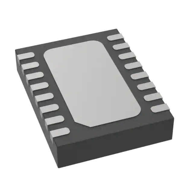
- Part No.:
- LTC2381CDE-16#TRPBF
- Manufacturer:
- Analog Devices Inc.
- Category:
- Analog to Digital Converters (ADC)
- Package:
- 16-WFDFN Exposed Pad
- Datasheet:
-
 LTC2381CDE-16#TRPBF.pdf
- Description:
- IC ADC 16BIT SAR 16DFN
- Quantity:
- Payment:

- Shipping:

Inventory:4,949
Please send an inquiry. Send us your inquiry, and we will respond immediately.
Product details
Overview
LTC2381CDE-16#TRPBF from Analog Devices (acquired Linear Technology) is a 16-bit, 250ksps successive approximation register (SAR) analog-to-digital converter with fully differential ±2.5V input range, 92dB SNR at 20kHz, ±2LSB INL max, and 3.25mW power consumption at full throughput. It operates from a single 2.5V VDD supply and supports 1.8V–5V I/O logic levels via separate OVDD, enabling direct interfacing with diverse host processors in portable instrumentation and industrial data acquisition systems.
For engineers reviewing the LTC2381CDE-16#TRPBF datasheet, LTC2381CDE-16#TRPBF pinout, LTC2381CDE-16#TRPBF application, or LTC2381CDE-16#TRPBF equivalent, key selection considerations include guaranteed 16-bit no-missing-codes operation, extended 3.25µs acquisition time for low-power driver compatibility, daisy-chain SPI interface support, internal conversion clock, and operation across 0°C to 70°C ambient temperature.
Technical Context
The LTC2381CDE-16#TRPBF implements a proprietary sampling architecture that allows acquisition of the next sample during the current conversion cycle, eliminating pipeline delay and achieving zero-cycle latency. Its differential SAR core uses a 16-bit CDAC and high-precision comparator referenced to an external 2.5V source, delivering bipolar 2's complement output codes with 76µV LSB resolution.
Conversion timing is governed by an internal oscillator, fixing tCONV at 2–3µs and enabling precise, jitter-free sampling at up to 250ksps. The device automatically powers down between conversions, scaling quiescent current from 1.7mA at 250ksps to 0.5µA in power-down mode - critical for battery-operated systems requiring dynamic power management.
Key Specifications
| Parameter | Value and Actual Design Meaning |
|---|---|
| Resolution | 16-bit - guarantees monotonic transfer function and full 65,536-code dynamic range without missing codes. |
| Sampling Rate | 250ksps - enables real-time capture of signals up to 125kHz Nyquist bandwidth with no latency between samples. |
| INL (Max) | ±2LSB - ensures end-point linearity error remains within ±0.03% of full scale, supporting precision measurement applications. |
| SNR (Typ) | 92dB at fIN = 20kHz - corresponds to effective resolution of ~15.0 bits and <100µVRMS noise floor in 20kHz bandwidth. |
| Power (250ksps) | 3.25mW - achieved with 2.5V VDD and 2.5V OVDD; enables thermal design in space-constrained DFN packages. |
| Input Range | ±2.5V fully differential - accepts true bipolar signals directly; common-mode range centered at VREF/2 = 1.25V. |
| Acquisition Time | 3.25µs - allows use of ultra-low-power op-amps (e.g., LT6350) with relaxed settling requirements, reducing system power budget. |
Pinout & Package
Package: 16-lead (4mm × 3mm) plastic DFN with exposed pad (Pin 17), rated for 0°C to 70°C operation. Exposed pad must be soldered to PCB ground plane for thermal and electrical performance.
| Pin/Terminal | Circuit Role | Design Meaning |
|---|---|---|
| IN+, IN– | Differential analog inputs | Accept ±2.5V differential signal; input capacitance 45pF in sample mode; require matched drive impedance for optimal CMRR. |
| REF (Pins 7, 8) | External reference voltage input | Accepts 2.4V–2.6V source; draws up to 285µA DC load at 250ksps; requires 47µF X5R ceramic bypass capacitor. |
| VDD (Pin 2) | Digital core supply | 2.375V–2.625V at 2.5V nominal; supplies ADC logic and CDAC; bypass with 10µF ceramic capacitor. |
| OVDD (Pin 15) | I/O interface supply | 1.71V–5.25V; sets logic thresholds for SDO, SCK, RDL/SDI, BUSY; decouple with 0.1µF ceramic capacitor. |
| CNV (Pin 9) | Convert trigger input | Rising-edge initiated conversion; high level maintains auto power-down between conversions. |
| BUSY (Pin 11) | Conversion status indicator | Active-high open-drain output; asserts during conversion; used for timing synchronization or interrupt generation. |
| SDO (Pin 14) | Serial data output | 2's complement 16-bit result; MSB-first; tri-state controlled by RDL/SDI when CHAIN = low. |
| SCK (Pin 13) | Serial clock input | Drives data shift-out on rising edge; supports up to 100MHz clock rate (10ns period); timing-critical for setup/hold compliance. |
| RDL/SDI (Pin 12) | Read enable / serial data input | When CHAIN = low: bus enable control for SDO tri-state; when CHAIN = high: SDI for daisy-chain configuration. |
| CHAIN (Pin 1) | Interface mode selector | High = daisy-chain mode (RDL/SDI becomes SDI); low = normal mode (RDL/SDI controls SDO output enable). |
Key Features
| Feature | Design Value |
|---|---|
| No pipeline delay, zero cycle latency | Enables deterministic real-time control loops and eliminates post-processing correction for time-critical sampling. |
| Extended 3.25µs acquisition window | Reduces required op-amp slew rate and bandwidth, allowing use of sub-10MHz GBW drivers like LT6350 to maintain 92dB SNR. |
| 1.8V–5V I/O voltage support (OVDD) | Eliminates level-shifting components when interfacing with FPGA, MCU, or DSP operating at mixed logic voltages. |
| Daisy-chain SPI mode | Supports multi-ADC synchronization with single SCK/SCK chain and shared CNV, reducing PCB routing complexity and controller GPIO count. |
| Internal conversion clock | Removes need for external clock generator or crystal; simplifies layout and improves jitter immunity in noisy environments. |
| Auto power-down between conversions | Reduces average power by >99% during idle periods; enables 13µW operation at 1ksps for battery-powered logging applications. |
Applications
| Portable Instrumentation | Industrial Process Control |
|---|---|
Use Scenario: Handheld multimeter or portable oscilloscope capturing transient waveforms in field service environments. IC Role / Device Role / Timing Role: Primary high-resolution digitizer acquiring ±2.5V sensor outputs (e.g., strain gauge bridges, thermocouples) at 250ksps with minimal latency. Use Value: 92dB SNR and ±2LSB INL ensure accurate RMS, harmonic, and distortion measurements; 3.25mW power enables >8-hour battery life. |
Use Scenario: Distributed I/O module monitoring pressure, flow, and temperature in factory automation PLC racks. IC Role / Device Role / Timing Role: Precision analog front-end for isolated sensor channels, synchronized via shared CNV and daisy-chained SPI. Use Value: Guaranteed 16-bit no-missing-codes operation over 0°C–70°C ensures reliable calibration traceability; daisy-chain reduces wiring and controller overhead. |
| Medical Imaging Subsystem | Automated Test Equipment (ATE) |
Use Scenario: Ultrasound beamformer channel digitizing echo return signals in portable imaging probes. IC Role / Device Role / Timing Role: High-speed, low-noise ADC capturing narrowband RF envelope signals with precise timing alignment across multiple channels. Use Value: 30ps aperture jitter and 92dB SNR preserve signal fidelity for Doppler shift analysis; internal clock eliminates external jitter sources. |
Use Scenario: Parametric test head measuring DC accuracy and AC performance of semiconductor devices under test. IC Role / Device Role / Timing Role: Reference-grade digitizer validating DUT output linearity, noise, and THD with calibrated ±2.5V input range. Use Value: ±2LSB INL and 92dB SNR meet Class A ATE accuracy requirements; 250ksps throughput supports rapid production test cycles. |
Equivalent & Alternatives
The following parts are listed as comparable options for similar high-speed SAR ADC applications.
| Alternative Part | Technical Difference | Application Difference | Selection Advice |
|---|---|---|---|
| AD7960BCPZ-RL7 | 18-bit, 5MSPS, 2.5V supply, ±2.5V input, but requires external reference and clock; higher power (34mW at 5MSPS). | Higher resolution/speed for lab-grade instrumentation; less suitable for portable or thermally constrained designs. | Select when 18-bit resolution and 5MSPS throughput outweigh power and BOM cost constraints. |
| ADS8860IRGET | 16-bit, 1MSPS, 2.5–5V supply, pseudo-differential input (single-ended IN+ with IN– tied to VREF/2), no daisy-chain mode. | Lower cost for single-ended sensor interfaces; lacks true differential input and daisy-chain capability. | Select for cost-sensitive, single-ended applications where 1MSPS is sufficient and differential rejection is not required. |
Compared with AD7960BCPZ-RL7 and ADS8860IRGET, the LTC2381CDE-16#TRPBF uniquely balances 250ksps speed, true differential input, daisy-chain SPI, and ultra-low 3.25mW power in a compact DFN - making it optimal for portable, multi-channel, and thermally sensitive precision data acquisition.
Availability
LTC2381CDE-16#TRPBF is available at Aetrix Electronics and suitable for portable instrumentation, industrial process control, and automated test equipment requiring stable component supply, long-term lifecycle assurance, and RoHS-compliant packaging.
Supply support for LTC2381CDE-16#TRPBF includes scheduled delivery planning, volume procurement assistance, BOM continuity management, traceable sourcing, and lifecycle availability coordination for OEM customers, industrial embedded developers, connected-device designers, and electronics production programs.
Manufacturer
Analog Devices, Inc. (ADI) is a global leader in high-performance analog, mixed-signal, and digital signal processing technologies, formed through the acquisition of Linear Technology in 2017.
The LTC2381-16 belongs to ADI's precision SAR ADC product line, designed specifically for applications demanding high resolution, low power, and zero-latency sampling in space- and energy-constrained systems - including portable medical devices, industrial sensors, and test instrumentation.
FAQ
What is the operating temperature range for the LTC2381CDE-16#TRPBF?
The LTC2381CDE-16#TRPBF is specified for operation from 0°C to 70°C ambient temperature. This commercial-grade rating applies to the DFN package variant marked "C" in the part number. For extended temperature ranges, consider the I-grade (–40°C to 85°C) or H-grade (–40°C to 125°C) MSOP variants.
Does the LTC2381CDE-16#TRPBF require an external clock source?
No, the LTC2381CDE-16#TRPBF features an internal conversion clock, eliminating the need for an external oscillator or clock generator. This simplifies system design, reduces component count, and improves jitter immunity - all while maintaining guaranteed 250ksps throughput and 2–3µs conversion time.
Can the LTC2381CDE-16#TRPBF interface directly with a 1.8V microcontroller?
Yes. The LTC2381CDE-16#TRPBF supports 1.8V–5V logic levels via its dedicated OVDD supply pin (Pin 15). When OVDD is set to 1.8V, all digital I/O pins (SDO, SCK, RDL/SDI, BUSY) operate at compatible voltage thresholds, enabling direct connection to 1.8V MCUs without level shifters.
What reference voltage is recommended for the LTC2381CDE-16#TRPBF?
The LTC2381CDE-16#TRPBF requires a stable 2.5V external reference. The LTC6652-2.5 is explicitly recommended in the datasheet: it delivers 0.05% initial accuracy, 5ppm/°C drift, and is specified over the full H-grade temperature range - ensuring optimal SNR and INL performance across the operating range.
How does the daisy-chain mode work on the LTC2381CDE-16#TRPBF?
In daisy-chain mode (CHAIN pin high), the RDL/SDI pin functions as SDI, accepting serial data from the previous ADC in the chain. Multiple LTC2381CDE-16#TRPBF devices can share one SCK and CNV line, with SDO of each feeding SDI of the next - enabling synchronized multi-channel acquisition with minimal controller resources.
LTC2381CDE-16#TRPBF Specifications
- Product attributes
- Attribute value
- Manufacturer:
- Analog Devices Inc.
- Series:
- -
- Package/Case:
- 16-WFDFN Exposed Pad
- Packaging:
- Tape & Reel (TR)
- Product Status:
- Active
- Number of Bits:
- 16
- Sampling Rate (Per Second):
- 250k
- Number of Inputs:
- 1
- Input Type:
- Differential
- Data Interface:
- SPI
- Configuration:
- S/H-ADC
- Ratio - S/H:ADC:
- 1:1
- Number of A/D Converters:
- 1
- Architecture:
- SAR
- Reference Type:
- External
- Voltage - Supply, Analog:
- 2.375V ~ 2.625V
- Voltage - Supply, Digital:
- 2.375V ~ 2.625V
- Features:
- -
- Operating Temperature:
- 0°C ~ 70°C
- Supplier Device Package:
- 16-DFN (4x3)
- Mounting Type:
- Surface Mount
- Grade:
- -
- Qualification:
- -
LTC2381CDE-16#TRPBF FAQ
1.How can I place an order for LTC2381CDE-16#TRPBF through Aetrix?
Please submit a Request for Quotation (RFQ) for LTC2381CDE-16#TRPBF on Aetrix. Our sales agent will provide a competitive quotation and guide you through the order confirmation once you accept the terms.
2.Are the price and stock information for LTC2381CDE-16#TRPBF reliable?
The price and inventory of LTC2381CDE-16#TRPBF are updated periodically and may fluctuate due to market conditions. Stock and pricing data are typically refreshed every 24 hours. Quotation validity for LTC2381CDE-16#TRPBF is usually 5 days.
3.What payment methods are accepted for LTC2381CDE-16#TRPBF?
We accept Wire Transfer, PayPal, Credit Card, Western Union, MoneyGram, and Escrow for LTC2381CDE-16#TRPBF transactions.
Note: Certain payment methods may incur a processing fee.
4.How is shipping managed for LTC2381CDE-16#TRPBF?
LTC2381CDE-16#TRPBF orders can be shipped via leading logistics carriers, including DHL, UPS, FedEx, TNT, or Registered Mail.
Once your LTC2381CDE-16#TRPBF order is processed, you will receive an email with the shipment details and tracking number.
Note: Tracking information may take up to 24 hours to appear. Express delivery typically takes 3–5 business days.
5.How can I obtain technical support or documentation for LTC2381CDE-16#TRPBF?
For technical support, including LTC2381CDE-16#TRPBF datasheets, pinout diagrams, or application guidance, please contact our engineering support team. They can provide detailed documentation and assistance for your LTC2381CDE-16#TRPBF requirements.
6.How does Aetrix verify that LTC2381CDE-16#TRPBF is sourced from the original manufacturer or authorized distributors?
All LTC2381CDE-16#TRPBF products on Aetrix are procured from qualified distributors and authorized channels. Our dedicated quality assurance team conducts strict verification, including traceability checks and, if necessary, third-party testing. This ensures that LTC2381CDE-16#TRPBF meets industry standards.
7.What is the process for return or replacement of LTC2381CDE-16#TRPBF?
All LTC2381CDE-16#TRPBF units undergo pre-shipment inspection (PSI). If there is an issue with LTC2381CDE-16#TRPBF, returns or replacements are accepted under the following conditions:
1.Quantity discrepancies, incorrect items, or visible external defects (such as breakage or corrosion), acknowledged by Aetrix.
2.The issue is reported within 90 days of delivery.
3.The LTC2381CDE-16#TRPBF part is unused and in its original packaging.
Return procedure for LTC2381CDE-16#TRPBF:
1.Submit a request within 90 days.
2.Obtain a Return Material Authorization (RMA) from Aetrix.
LTC2381CDE-16#TRPBF Tags
-
ADC081C021CIMKX/NOPB
Texas Instruments

-
MCP3021A5T-E/OT
Microchip Technology
-
TLA2024IRUGR
Texas Instruments
-
MCP3221A5T-E/OT
Microchip Technology
-
MCP3221A5T-I/OT
Microchip Technology
-
MCP3221A4T-E/OT
Microchip Technology
-
MCP3221A6T-E/OT
Microchip Technology
-
MCP3221A0T-E/OT
Microchip Technology
-
MCP3221A1T-E/OT
Microchip Technology

-
ADC121S021CIMFX/NOPB
Texas Instruments

-
MCP3001-I/MS
Microchip Technology

-
MCP3001-I/SN
Microchip Technology
Tech Hub

A practical engineering guide to 3.3V and 5V logic compatibility, input thresholds, resistor dividers, translator ICs, MOSFET level shifting, I2C pull-ups, timing limits and power-sequencing risks.

The 74HC595 uses push-pull logic outputs, while the TPIC6B595 uses 50 V open-drain DMOS sinks for higher-power loads. This guide compares timing, current limits, 3.3 V interfacing, load wiring, thermal…

The 74HC595 converts serial data into eight stable parallel outputs. This guide covers pin functions, shift and storage timing, OE and MR behavior, drive-current limits, cascading, voltage compatibilit…

A technical comparison of level-sensitive latches and edge-triggered flip-flops, covering timing windows, setup and hold limits, master–slave operation, time borrowing, race-through, HDL inference and…

A D latch stores one bit while Enable controls when data can pass. This reference covers gate-level operation, truth tables, transparency, setup and hold timing, LE versus OE, common ICs and practical …

An SR latch stores one bit through cross-coupled feedback. This engineering reference covers NOR and NAND implementations, truth tables, forbidden-state recovery, gated operation, switch debouncing, fa…

Latch circuits retain one bit through feedback. This technical reference covers SR and D latches, truth tables, transparency, timing limits, latch-versus-flip-flop behavior, applications and common log…

An engineering guide to LED driver operation, constant-current and constant-voltage outputs, linear and switching topologies, dimming, IC selection, calculations, replacement compatibility, and fault c…

Operational amplifier guide covering op amp basics, feedback, ideal vs real op amps, common configurations, buffer circuits, offset, bias current, gain-bandwidth, slew rate, rail-to-rail limits and sel…

Jumper cables guide covering safe connection order, red and black clamp placement, final ground connection, cable gauge, length, clamp quality, copper vs CCA cables, jump starter comparison and battery…


