
 My Inquiry
 My Account


Analog Devices Inc. LTC2913CDD-1#TRPBF
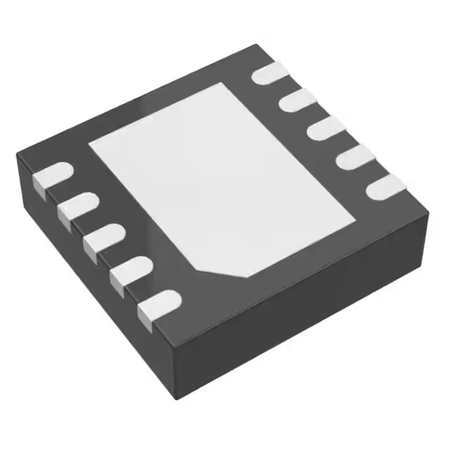
- Part No.:
- LTC2913CDD-1#TRPBF
- Manufacturer:
- Analog Devices Inc.
- Category:
- Supervisors
- Package:
- 10-WFDFN Exposed Pad
- Datasheet:
-
 LTC2913CDD-1#TRPBF.pdf
- Description:
- IC SUPERVISOR 2 CHANNEL 10DFN
- Quantity:
- Payment:

- Shipping:

Inventory:2,909
Please send an inquiry. Send us your inquiry, and we will respond immediately.
Product details
Overview
LTC2913CDD-1#TRPBF from Analog Devices (acquired Linear Technology) is a dual-input, latching overvoltage/undervoltage supervisor IC for precision supply monitoring in multi-rail systems. It monitors two independent voltage rails with adjustable UV/OV thresholds (±1.5% accuracy), features open-drain UV/OV outputs, 44μA quiescent current, and operates down to VCC = 1V. Used in desktop/notebook computers and network servers for core/I/O rail supervision.
For engineers reviewing the LTC2913CDD-1#TRPBF datasheet, LTC2913CDD-1#TRPBF pinout, LTC2913CDD-1#TRPBF application, or LTC2913CDD-1#TRPBF equivalent, key selection considerations include its latching OV output (LTC2913-1 variant), 10-lead DFN (3mm × 3mm) package, TMR-adjustable timeout (6–14ms), guaranteed operation at VCC ≥ 1V, and ±1.5% threshold accuracy across 0°C to 70°C.
Technical Context
The LTC2913CDD-1#TRPBF implements dual independent comparator pairs (VH1/VL1 and VH2/VL2), each detecting undervoltage (VHn < 0.5V) and overvoltage (VLn > 0.5V) conditions. All comparators share a common 0.5V internal reference and feed into a single UV output and a latched OV output.
Its timing architecture includes a programmable reset timeout (tUOTO = 6–14ms with CTMR = 1nF), glitch-filtered inputs rejecting transients below the curve in Figure 2913 G05, and a dedicated LATCH pin (Pin 8) that enables OV latching when pulled low - a defining feature of the -1 variant.
Key Specifications
| Parameter | Value and Actual Design Meaning |
|---|---|
| VCC Range | 2.3V to 6V direct supply; shunt-regulated operation above 6V with external current-limiting resistor |
| Threshold Accuracy | ±1.5% over full temperature range - ensures reliable reset triggering within tight supply tolerance bands |
| Quiescent Current | 44μA typical - enables micropower system-level monitoring without burdening low-power rails |
| UV/OV Output Type | Open-drain with weak internal pull-up to VCC - supports wired-OR configurations and flexible external pull-up selection |
| Reset Timeout (tUOTO) | 6–14ms (typ. 8.5ms @ CTMR = 1nF) - guarantees minimum reset pulse width for stable power sequencing |
| Operating Temp | 0°C to 70°C (C-grade) - validated for commercial computing and server environments |
| Input Glitch Rejection | Integrated low-pass filtering on all VH/VL inputs - prevents false resets from sub-μs noise transients |
Pinout & Package
Package: 10-lead (3mm × 3mm) plastic DFN with exposed pad (Pin 11, optional GND connection).
| Pin/Terminal | Circuit Role | Design Meaning |
|---|---|---|
| VH1 (Pin 1) | Undervoltage sense input 1 | Asserts UV when voltage drops below 0.5V; tied to high-side divider tap for positive rail monitoring |
| VL1 (Pin 2) | Overvoltage sense input 1 | Asserts OV when voltage rises above 0.5V; tied to low-side divider tap for same rail |
| VH2 (Pin 3) | Undervoltage sense input 2 | Independent second UV channel - enables concurrent monitoring of dual supplies (e.g., 5V & 3.3V) |
| VL2 (Pin 4) | Overvoltage sense input 2 | Independent second OV channel - supports fault isolation across separate power domains |
| GND (Pin 5) | Device ground reference | Return path for all internal circuitry and external timing capacitor (CTMR) |
| OV (Pin 6) | Latched overvoltage logic output | Open-drain output asserted low on OV condition; remains latched until LATCH pin is pulled high |
| UV (Pin 7) | Undervoltage logic output | Open-drain output asserted low on any VHn undervoltage; held low for tUOTO after recovery |
| LATCH (Pin 8) | OV latch clear/bypass control | Pull low to enable OV latching; pull high to clear latch and revert OV to non-latching behavior |
| TMR (Pin 9) | Reset timeout timer input | Connect external capacitor (≥10pF) to GND to set tUOTO; tie to VCC to bypass timeout |
| VCC (Pin 10) | Supply input / shunt regulator | Accepts 2.3–6V directly; regulates >6V supplies via internal 6.6V shunt (max 10mA input current) |
Key Features
| Feature | Design Value |
|---|---|
| Dual independent UV/OV monitoring channels | Enables simultaneous supervision of two critical rails (e.g., CPU core + I/O) with shared outputs and timing |
| Latching OV output (LTC2913-1 variant) | Ensures persistent fault indication until explicitly cleared - critical for diagnostics and fail-safe system states |
| Adjustable reset timeout via external capacitor | Supports precise power-on reset timing (6–14ms typical) without requiring internal RC trimming or calibration |
| Guaranteed operation down to VCC = 1V | Provides valid UV assertion and OV blocking during brown-out conditions - essential for robust power-down sequencing |
| ±1.5% threshold accuracy over temperature | Minimizes design margin overhead and eliminates need for external calibration in commercial-grade applications |
Applications
| Desktop Computer Power Management | Notebook System Voltage Supervision |
|---|---|
Use Scenario: Monitoring 12V main input and 5V/3.3V secondary rails during cold start and thermal throttling events. IC Role / Device Role / Timing Role: Dual-channel UV/OV supervisor asserting system reset if either rail falls below 4.5V (5V rail) or exceeds 5.5V, with latched OV for post-fault analysis. Use Value: Prevents corrupted BIOS writes and memory initialization errors by enforcing strict power-good windows before CPU release. |
Use Scenario: Supervising battery-charged 5V and USB-powered 3.3V rails in dual-source power architectures. IC Role / Device Role / Timing Role: Independent VH1/VL1 and VH2/VL2 inputs track both rails; LATCH pin enables firmware-controlled OV fault clearing after battery swap. Use Value: Eliminates spurious reboots during dynamic source switching while maintaining deterministic reset timing via TMR capacitor. |
| Network Server Core Voltage Monitoring | Industrial Embedded Controller Supply Integrity |
Use Scenario: Validating 1.8V FPGA core and 1.2V SoC I/O voltages under load-step transients in 1U rack servers. IC Role / Device Role / Timing Role: Uses internal 0.5V reference and external resistor dividers to detect UV at 1.71V (±5%) and OV at 1.89V; tUOTO holds reset for 200ms (CTMR = 22nF) to allow rail settling. Use Value: Guarantees clean FPGA configuration and DDR initialization by preventing release until all rails stabilize post-transient. |
Use Scenario: Ensuring safe operation of PLC I/O modules powered by isolated 24V DC and regulated 5V logic supplies. IC Role / Device Role / Timing Role: VH1/VL1 monitors 24V input for overvoltage (26.4V) and undervoltage (21.6V); VH2/VL2 supervises 5V logic rail; LATCH pin interfaces with watchdog MCU for fault logging. Use Value: Enables deterministic field-replaceable unit (FRU) detection and graceful shutdown upon sustained overvoltage - meeting IEC 61000-4-5 surge immunity requirements. |
Equivalent & Alternatives
The following parts are listed as comparable options for similar dual-supply monitoring applications.
| Alternative Part | Technical Difference | Application Difference | Selection Advice |
|---|---|---|---|
| LTC2914CMS#PBF | Quad UV/OV monitor (4 inputs), 16-lead MSOP, supports negative voltage monitoring via external resistors | Required for systems needing >2 monitored rails or mixed positive/negative supplies (e.g., op-amp bias rails) | Select LTC2914 when expanding beyond dual-rail monitoring or adding negative rail support - not drop-in compatible due to pin count and function expansion |
| LTC2904CMS8#PBF | 3-state programmable dual supply monitor; adjustable tolerance (0.5–5%), no latching OV, 8-lead SOT-23 | Suitable for cost-sensitive, space-constrained designs where latching is unnecessary and tighter tolerance tuning is required | Choose LTC2904 for compact, non-latching dual-rail supervision with user-defined trip margins - differs in package, pinout, and lack of latch functionality |
Compared with LTC2913CDD-1#TRPBF, LTC2914 offers expanded channel count and negative rail capability at the cost of larger footprint and higher complexity, while LTC2904 provides smaller size and adjustable tolerance but omits latching and requires different PCB layout and timing configuration.
Availability
LTC2913CDD-1#TRPBF is available at Aetrix Electronics and suitable for desktop computers, network servers, and embedded industrial controllers requiring stable component supply with guaranteed commercial-temperature performance and long-term lifecycle support.
Supply support for LTC2913CDD-1#TRPBF includes scheduled delivery planning, volume procurement assistance, BOM continuity management, traceable sourcing, and lifecycle availability coordination for OEM customers, industrial embedded developers, connected-device designers, and electronics production programs.
Manufacturer
Analog Devices, Inc. (ADI) acquired Linear Technology in 2017 and maintains its high-performance analog and power management portfolio, emphasizing precision, reliability, and low-power innovation.
The LTC2913 product line delivers micropower, high-accuracy voltage supervision for multi-rail digital systems - designed specifically for computing, communications, and industrial applications demanding robust power sequencing and fault logging.
FAQ
What is the key functional difference between LTC2913CDD-1#TRPBF and LTC2913CDD-2#TRPBF?
The LTC2913CDD-1#TRPBF features a latching overvoltage (OV) output controlled by the LATCH pin: pulling LATCH low causes OV to latch low on fault detection and remain asserted until LATCH is pulled high. In contrast, LTC2913CDD-2#TRPBF replaces LATCH with a DIS (disable) pin that disables both UV and OV outputs when driven high. This makes LTC2913CDD-1#TRPBF ideal for fault-hold applications, while LTC2913CDD-2#TRPBF suits scenarios requiring output blanking during maintenance or test modes.
How does the LTC2913CDD-1#TRPBF achieve ±1.5% threshold accuracy over temperature?
The LTC2913CDD-1#TRPBF achieves ±1.5% threshold accuracy by using a trimmed, temperature-compensated 0.5V internal reference voltage applied to all four comparator inputs (VH1, VL1, VH2, VL2). This reference is laser-trimmed during production and stabilized across –40°C to 125°C, ensuring consistent trip points regardless of ambient or supply variation. The specification applies to the internal 0.5V threshold itself - external resistor divider accuracy must be considered separately for overall system tolerance.
Can LTC2913CDD-1#TRPBF monitor a 12V supply directly, and what precautions are needed?
Yes, LTC2913CDD-1#TRPBF can monitor a 12V supply, but VCC must not exceed 6V directly. To power the IC from 12V, connect it through an external current-limiting resistor (RZ) to leverage the internal 6.6V shunt regulator. For example, with 12V input and max 10mA VCC current, RZ ≈ (12V – 6.6V)/10mA = 540Ω. The resistor must also handle power dissipation (≈54mW). VH1/VL1 and VH2/VL2 inputs remain safe up to 16V, so 12V may be applied directly to them via appropriate resistor dividers.
What is the minimum recommended capacitor value for the TMR pin on LTC2913CDD-1#TRPBF, and why?
The minimum recommended capacitor value for the TMR pin on LTC2913CDD-1#TRPBF is 10pF. This value ensures sufficient charge/discharge time for reliable timeout timing generation. Capacitors smaller than 10pF risk erratic or shortened timeout periods due to parasitic capacitance dominating the timing node. The datasheet specifies CTMR ≥ 10pF to guarantee predictable tUOTO behavior across process, voltage, and temperature variations - values like 1nF (yielding ~8.5ms timeout) or 22nF (~200ms) are commonly used for practical reset durations.
Does LTC2913CDD-1#TRPBF require external pull-up resistors on UV and OV outputs?
LTC2913CDD-1#TRPBF includes weak internal pull-ups to VCC on both UV and OV outputs, eliminating the need for external pull-ups in most cases. However, an external pull-up (≤100kΩ) is recommended on OV when operating at VCC < 2V, because the internal pull-up strength diminishes significantly below this voltage. External pull-ups are also necessary for wired-OR configurations or when faster rise times are required - though doing so increases total pull-up strength, requiring stronger pull-downs from other devices sharing the net.
LTC2913CDD-1#TRPBF Specifications
- Product attributes
- Attribute value
- Manufacturer:
- Analog Devices Inc.
- Series:
- -
- Package/Case:
- 10-WFDFN Exposed Pad
- Packaging:
- Tape & Reel (TR)
- Product Status:
- Active
- Programmable:
- Not Verified
- Type:
- Multi-Voltage Supervisor
- Number of Voltages Monitored:
- 2
- Voltage - Threshold:
- Adjustable/Selectable
- Output:
- Open Drain or Open Collector
- Reset:
- Active Low
- Reset Timeout:
- Adjustable/Selectable
- Operating Temperature:
- 0°C ~ 70°C (TA)
- Grade:
- -
- Qualification:
- -
- Mounting Type:
- Surface Mount
- Supplier Device Package:
- 10-DFN (3x3)
LTC2913CDD-1#TRPBF FAQ
1.How can I place an order for LTC2913CDD-1#TRPBF through Aetrix?
Please submit a Request for Quotation (RFQ) for LTC2913CDD-1#TRPBF on Aetrix. Our sales agent will provide a competitive quotation and guide you through the order confirmation once you accept the terms.
2.Are the price and stock information for LTC2913CDD-1#TRPBF reliable?
The price and inventory of LTC2913CDD-1#TRPBF are updated periodically and may fluctuate due to market conditions. Stock and pricing data are typically refreshed every 24 hours. Quotation validity for LTC2913CDD-1#TRPBF is usually 5 days.
3.What payment methods are accepted for LTC2913CDD-1#TRPBF?
We accept Wire Transfer, PayPal, Credit Card, Western Union, MoneyGram, and Escrow for LTC2913CDD-1#TRPBF transactions.
Note: Certain payment methods may incur a processing fee.
4.How is shipping managed for LTC2913CDD-1#TRPBF?
LTC2913CDD-1#TRPBF orders can be shipped via leading logistics carriers, including DHL, UPS, FedEx, TNT, or Registered Mail.
Once your LTC2913CDD-1#TRPBF order is processed, you will receive an email with the shipment details and tracking number.
Note: Tracking information may take up to 24 hours to appear. Express delivery typically takes 3–5 business days.
5.How can I obtain technical support or documentation for LTC2913CDD-1#TRPBF?
For technical support, including LTC2913CDD-1#TRPBF datasheets, pinout diagrams, or application guidance, please contact our engineering support team. They can provide detailed documentation and assistance for your LTC2913CDD-1#TRPBF requirements.
6.How does Aetrix verify that LTC2913CDD-1#TRPBF is sourced from the original manufacturer or authorized distributors?
All LTC2913CDD-1#TRPBF products on Aetrix are procured from qualified distributors and authorized channels. Our dedicated quality assurance team conducts strict verification, including traceability checks and, if necessary, third-party testing. This ensures that LTC2913CDD-1#TRPBF meets industry standards.
7.What is the process for return or replacement of LTC2913CDD-1#TRPBF?
All LTC2913CDD-1#TRPBF units undergo pre-shipment inspection (PSI). If there is an issue with LTC2913CDD-1#TRPBF, returns or replacements are accepted under the following conditions:
1.Quantity discrepancies, incorrect items, or visible external defects (such as breakage or corrosion), acknowledged by Aetrix.
2.The issue is reported within 90 days of delivery.
3.The LTC2913CDD-1#TRPBF part is unused and in its original packaging.
Return procedure for LTC2913CDD-1#TRPBF:
1.Submit a request within 90 days.
2.Obtain a Return Material Authorization (RMA) from Aetrix.
LTC2913CDD-1#TRPBF Tags
-
MIC826SYMT-TR
Microchip Technology

-
APX803S-31SA-7
Diodes Incorporated
-
APX803L20-29SA-7
Diodes Incorporated

-
TPS3828-33DBVR
Texas Instruments

-
V6340RSP3B+
EM Microelectronic
-
EM6325CXSP5B-2.9+
EM Microelectronic
-
MCP120T-300I/TT
Microchip Technology
-
MCP130T-315I/TT
Microchip Technology
-
MCP120T-475I/TT
Microchip Technology
-
MCP111T-300E/TT
Microchip Technology
-
MCP120T-315I/TT
Microchip Technology
-
MCP809T-315I/TT
Microchip Technology
Tech Hub

A practical engineering guide to 3.3V and 5V logic compatibility, input thresholds, resistor dividers, translator ICs, MOSFET level shifting, I2C pull-ups, timing limits and power-sequencing risks.

The 74HC595 uses push-pull logic outputs, while the TPIC6B595 uses 50 V open-drain DMOS sinks for higher-power loads. This guide compares timing, current limits, 3.3 V interfacing, load wiring, thermal…

The 74HC595 converts serial data into eight stable parallel outputs. This guide covers pin functions, shift and storage timing, OE and MR behavior, drive-current limits, cascading, voltage compatibilit…

A technical comparison of level-sensitive latches and edge-triggered flip-flops, covering timing windows, setup and hold limits, master–slave operation, time borrowing, race-through, HDL inference and…

A D latch stores one bit while Enable controls when data can pass. This reference covers gate-level operation, truth tables, transparency, setup and hold timing, LE versus OE, common ICs and practical …

An SR latch stores one bit through cross-coupled feedback. This engineering reference covers NOR and NAND implementations, truth tables, forbidden-state recovery, gated operation, switch debouncing, fa…

Latch circuits retain one bit through feedback. This technical reference covers SR and D latches, truth tables, transparency, timing limits, latch-versus-flip-flop behavior, applications and common log…

An engineering guide to LED driver operation, constant-current and constant-voltage outputs, linear and switching topologies, dimming, IC selection, calculations, replacement compatibility, and fault c…

Operational amplifier guide covering op amp basics, feedback, ideal vs real op amps, common configurations, buffer circuits, offset, bias current, gain-bandwidth, slew rate, rail-to-rail limits and sel…

Jumper cables guide covering safe connection order, red and black clamp placement, final ground connection, cable gauge, length, clamp quality, copper vs CCA cables, jump starter comparison and battery…


