
 My Inquiry
 My Account


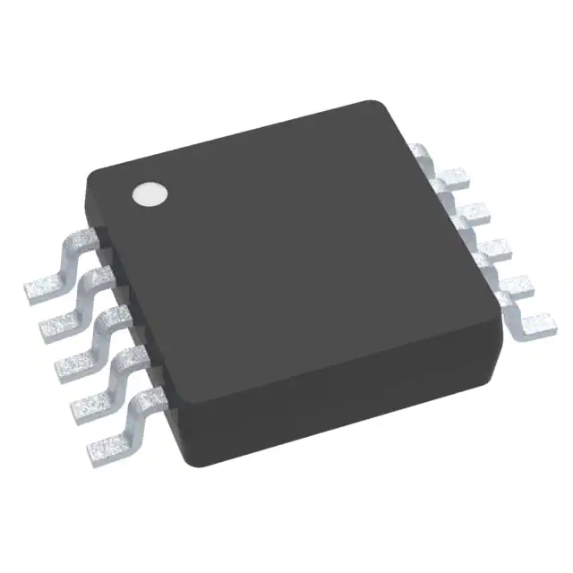
Analog Devices Inc. LTC2927CTS8#TRPBF
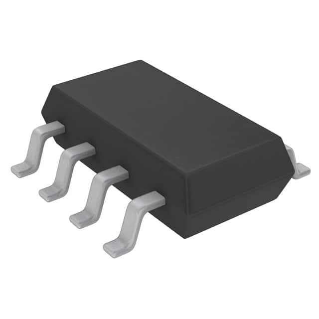
- Part No.:
- LTC2927CTS8#TRPBF
- Manufacturer:
- Analog Devices Inc.
- Category:
- Power Supply Controllers, Monitors
- Package:
- SOT-23-8 Thin, TSOT-23-8
- Datasheet:
-
 LTC2927CTS8#TRPBF.pdf
- Description:
- IC POWER SUPPLY CTRLR TSOT23-8
- Quantity:
- Payment:

- Shipping:

Inventory:1,214
Please send an inquiry. Send us your inquiry, and we will respond immediately.
Product details
Overview
LTC2927CTS8#TRPBF from Analog Devices (formerly Linear Technology) is a single-supply power tracking controller IC that enables precise ramp-up and ramp-down sequencing between multiple DC/DC supplies without inserting series pass elements. It delivers 0.8V TRACK reference, ±5% current mirror matching, 10μA RAMP pull-up/pull-down current, and operates from 2.9V to 5.5V VCC. It is used in FPGA and microprocessor VCORE/VI/O supply coordination where voltage offset, ratiometric, or delayed sequencing is required.
For engineers reviewing the LTC2927CTS8#TRPBF datasheet, LTC2927CTS8#TRPBF pinout, LTC2927CTS8#TRPBF application, or LTC2927CTS8#TRPBF equivalent, key selection criteria include guaranteed 0.8V TRACK voltage accuracy over temperature, open-loop current-mirror tracking architecture preserving slave supply stability, SDO-controlled shutdown output timing, and compatibility with TSOT-23-8 package layout constraints.
Technical Context
The LTC2927CTS8#TRPBF implements an open-loop current-mirror tracking cell that forces the TRACK pin to 0.8V and mirrors its current to the FB pin, enabling voltage-controlled ramping of a slave DC/DC converter's feedback node. Its ON pin (1.23V threshold, 75mV hysteresis) selects ramp direction, while RAMP and RAMPBUF pins support external capacitor-based ramp generation or external master signal injection.
It features a dedicated open-drain SDO output that asserts low until both VCC exceeds 2.5V and ON rises above 1.23V - enabling coordinated startup control of slave supply RUN/SS pins. The device presents high impedance at FB and TRACK after ramp completion, eliminating impact on slave supply regulation accuracy, transient response, or loop stability.
Key Specifications
| Parameter | Value and Actual Design Meaning |
|---|---|
| VCC Range | 2.9V to 5.5V - defines minimum input rail for reliable operation and UVLO release |
| TRACK Voltage | 0.77V to 0.82V at –1mA - sets precision reference for current-mirror-based tracking ratio |
| RAMP Current | ±10μA - determines ramp rate when driving external capacitor (e.g., 0.1μF → 100V/s) |
| ON Threshold | 1.210V to 1.250V - controls direction switching point with 30–150mV hysteresis for noise immunity |
| SDO Output | Open-drain, sinks ≥1mA - directly drives RUN/SS pin of slave DC/DC converters for sequenced enable |
| ICC (Quiescent) | 0.25mA to 1.2mA - ensures low overhead during active tracking and minimal bias current in idle state |
| Operating Temp | 0°C to 70°C - specifies commercial-grade thermal envelope for board-level reliability |
Pinout & Package
Package: 8-Lead Plastic TSOT-23 (3mm × 1.75mm), RoHS-compliant, lead-free finish. Exposed pad optional for thermal relief but not electrically connected.
| Pin/Terminal | Circuit Role | Design Meaning |
|---|---|---|
| VCC (Pin 1) | Supply Input | Power rail input with 2.9V–5.5V range and 2.5V UVLO threshold; requires 0.1μF local bypass |
| SDO (Pin 2) | Shutdown Output | Open-drain output asserting low until VCC > 2.5V AND ON > 1.23V - used to hold slave RUN/SS pin low |
| FB (Pin 3) | Feedback Control | Current-source output mirroring TRACK current to modulate slave DC/DC feedback node; clamped at 2.3V max |
| GND (Pin 4) | Ground Reference | Analog ground return for internal circuitry and external decoupling; connects to PCB ground plane |
| TRACK (Pin 5) | Tracking Reference | Servos to 0.8V; supplies mirrored current to FB; limited to <25pF capacitance to maintain stability |
| RAMPBUF (Pin 6) | Ramp Buffer Output | Low-impedance buffered copy of RAMP; drives resistive divider to TRACK; supports ≤2mA load |
| RAMP (Pin 7) | Ramp Input | Input to internal 10μA current source/sink; accepts external ramp signal or capacitor for programmable slope |
| ON (Pin 8) | Direction Control | Digital or analog input controlling ramp direction; 1.23V threshold with hysteresis enables robust edge detection |
Key Features
| Feature | Design Value |
|---|---|
| Open-loop tracking | Preserves slave supply stability and transient response by avoiding feedback loop injection |
| Adjustable ramp rate | Set via external RAMP capacitor and 10μA current source - enables precise timing control (e.g., 10ms delay = 100mV @ 100V/s) |
| 0.8V TRACK reference | Guaranteed 0.77V–0.82V over full temp range - establishes accurate current mirror baseline for ratio control |
| SDO-controlled sequencing | Enables hardware-coordinated startup of downstream supplies without MCU intervention |
| TSOT-23-8 footprint | Compact 3mm × 1.75mm package - minimizes PCB area at point-of-load while supporting manual rework |
Applications
| VCORE/VI/O Supply Coordination | FPGA Power Sequencing |
|---|---|
Use Scenario: Coordinating 1.8V I/O and 1.0V core rails in Xilinx Artix-7 FPGA to prevent latch-up during power-up. IC Role / Device Role / Timing Role: LTC2927CTS8#TRPBF acts as master-tracking controller, generating synchronized ramps with fixed 0.8V offset between rails using RAMPBUF–TRACK resistor network. Use Value: Eliminates need for discrete RC timers or complex CPLD logic; guarantees <±50mV inter-rail differential during ramp transitions per JEDEC JESD8-12. | Use Scenario: Enabling 3.3V configuration supply before 1.2V transceiver and 0.85V logic rails in Intel Agilex FPGA systems. IC Role / Device Role / Timing Role: LTC2927CTS8#TRPBF provides delayed ramp initiation via RTA resistor network, enforcing strict power-on order per FPGA vendor spec. Use Value: Prevents configuration corruption and I/O contention by ensuring configuration rail reaches 90% before transceiver enable, verified with oscilloscope ramp capture. |
| Microprocessor Dual-Rail Tracking | Point-of-Load Supply Ratiometric Control |
Use Scenario: Managing 1.1V CPU core and 1.8V memory interface supplies in ARM Cortex-A72 SoC designs. IC Role / Device Role / Timing Role: LTC2927CTS8#TRPBF implements ratiometric ramping where memory rail rises at 85V/s while core rail rises at 60V/s, driven by independent RAMPBUF–TRACK dividers. Use Value: Maintains safe voltage margin (<1.2V) across all operating conditions, satisfying SoC absolute maximum ratings during dynamic load steps. | Use Scenario: Controlling dual 12V/5V isolated DC/DC modules in industrial PLC backplane where 5V must track 12V at 0.417× ratio. IC Role / Device Role / Timing Role: LTC2927CTS8#TRPBF serves as analog ratio engine - RAMPBUF voltage scaled via RTA/RTB sets TRACK current to force 5V output proportional to 12V master. Use Value: Replaces digital PMBus sequencing with deterministic analog behavior unaffected by firmware resets or communication latency. |
Equivalent & Alternatives
The following parts are listed as comparable options for similar power supply tracking applications.
| Alternative Part | Technical Difference | Application Difference | Selection Advice |
|---|---|---|---|
| TPS65023RGZR | Integrated triple-buck PMIC with built-in sequencing logic; no external RAMP capacitor needed but fixed internal timing. | Best for compact, low-component-count designs where all rails are generated internally; unsuitable for hybrid systems with external DC/DCs. | Select TPS65023RGZR when consolidating power delivery and reducing BOM count outweighs flexibility in ramp slope and offset tuning. |
| ADM1166ACPZ | Hot-swap and sequencing supervisor with 12-bit DAC-controlled ramp; requires I²C interface and firmware configuration. | Preferred for systems needing programmable, multi-event sequencing (e.g., pre-charge, soft-start, delay) beyond simple two-rail tracking. | Choose ADM1166ACPZ when field-upgradable sequencing profiles or integration with system management controllers are required. |
Compared with TPS65023RGZR and ADM1166ACPZ, the LTC2927CTS8#TRPBF offers analog-determined ramp behavior with zero firmware dependency, minimal external components, and direct current-mirror coupling to existing DC/DC feedback nodes - making it optimal for retrofitting tracking into legacy power architectures.
Availability
LTC2927CTS8#TRPBF is available at Aetrix Electronics and suitable for FPGA power sequencing, microprocessor dual-rail coordination, and industrial point-of-load supply ratiometric control requiring stable component supply and long-term production continuity.
Supply support for LTC2927CTS8#TRPBF includes scheduled delivery planning, volume procurement assistance, BOM continuity management, traceable sourcing, and lifecycle availability coordination for OEM customers, industrial embedded developers, connected-device designers, and electronics production programs.
Manufacturer
Analog Devices, Inc. (ADI) is a global leader in high-performance analog, mixed-signal, and digital signal processing semiconductors, formed through the acquisition of Linear Technology in 2017.
The LTC2927CTS8#TRPBF belongs to ADI's Power Management portfolio, specifically designed for analog-controlled power supply tracking and sequencing in space-constrained, high-reliability embedded systems where deterministic timing and stability preservation are critical.
FAQ
What is the function of the TRACK pin on the LTC2927CTS8#TRPBF?
The TRACK pin on the LTC2927CTS8#TRPBF serves as the precision 0.8V reference node for the internal current mirror. It sources or sinks current based on the voltage difference between RAMPBUF and TRACK, and that current is mirrored to the FB pin to control the slave DC/DC output. Its guaranteed 0.77V–0.82V range over temperature ensures consistent tracking ratio accuracy in the LTC2927CTS8#TRPBF.
Can the LTC2927CTS8#TRPBF be used to control more than one slave supply?
Yes, the LTC2927CTS8#TRPBF can control multiple slave supplies by replicating the RAMPBUF–TRACK–FB resistor network for each output. Each slave requires its own set of RTA, RTB, RFA, and RFB resistors to configure independent ramp rates, offsets, or delays. The LTC2927CTS8#TRPBF itself remains a single-master controller - one device per slave rail - but multiple LTC2927CTS8#TRPBF units can share the same RAMP signal for synchronized operation.
Does the LTC2927CTS8#TRPBF affect the stability of the slave DC/DC converter?
No, the LTC2927CTS8#TRPBF does not affect the stability of the slave DC/DC converter because it uses an open-loop current-mirror architecture. It injects controlled current into the FB node without altering the feedback loop's phase margin or gain characteristics. The LTC2927CTS8#TRPBF presents high impedance after ramp completion and avoids series pass elements - preserving the original compensation design of the slave supply.
What is the maximum recommended capacitance on the TRACK pin of the LTC2927CTS8#TRPBF?
The maximum recommended capacitance on the TRACK pin of the LTC2927CTS8#TRPBF is less than 25pF. Exceeding this value risks instability in the current-mirror servo loop, potentially causing oscillation or inaccurate ramp tracking. Layout best practices include minimizing trace length to the TRACK node and avoiding nearby noisy signals or ground vias that could couple parasitic capacitance into the LTC2927CTS8#TRPBF TRACK path.
How does the SDO pin of the LTC2927CTS8#TRPBF coordinate with the ON and VCC pins during startup?
During startup, the SDO pin of the LTC2927CTS8#TRPBF remains low until both conditions are met: VCC exceeds 2.5V (UVLO release) and the ON pin voltage rises above 1.23V. Once both are satisfied, SDO releases and goes high-impedance, allowing the connected slave supply's RUN/SS pin to be pulled up by its internal pull-up or external resistor. If either VCC drops below 2.5V or ON falls below ~1.225V (1.23V minus hysteresis), SDO actively pulls low again - ensuring tight hardware-enforced sequencing in the LTC2927CTS8#TRPBF.
LTC2927CTS8#TRPBF Specifications
- Product attributes
- Attribute value
- Manufacturer:
- Analog Devices Inc.
- Series:
- -
- Package/Case:
- SOT-23-8 Thin, TSOT-23-8
- Packaging:
- Tape & Reel (TR)
- Product Status:
- Active
- Programmable:
- Not Verified
- Applications:
- Power Supply Controller
- Voltage - Input:
- -
- Voltage - Supply:
- 2.9V ~ 5.5V
- Current - Supply:
- 560 µA
- Operating Temperature:
- 0°C ~ 70°C
- Grade:
- -
- Qualification:
- -
- Mounting Type:
- Surface Mount
- Supplier Device Package:
- TSOT-23-8
LTC2927CTS8#TRPBF FAQ
1.How can I place an order for LTC2927CTS8#TRPBF through Aetrix?
Please submit a Request for Quotation (RFQ) for LTC2927CTS8#TRPBF on Aetrix. Our sales agent will provide a competitive quotation and guide you through the order confirmation once you accept the terms.
2.Are the price and stock information for LTC2927CTS8#TRPBF reliable?
The price and inventory of LTC2927CTS8#TRPBF are updated periodically and may fluctuate due to market conditions. Stock and pricing data are typically refreshed every 24 hours. Quotation validity for LTC2927CTS8#TRPBF is usually 5 days.
3.What payment methods are accepted for LTC2927CTS8#TRPBF?
We accept Wire Transfer, PayPal, Credit Card, Western Union, MoneyGram, and Escrow for LTC2927CTS8#TRPBF transactions.
Note: Certain payment methods may incur a processing fee.
4.How is shipping managed for LTC2927CTS8#TRPBF?
LTC2927CTS8#TRPBF orders can be shipped via leading logistics carriers, including DHL, UPS, FedEx, TNT, or Registered Mail.
Once your LTC2927CTS8#TRPBF order is processed, you will receive an email with the shipment details and tracking number.
Note: Tracking information may take up to 24 hours to appear. Express delivery typically takes 3–5 business days.
5.How can I obtain technical support or documentation for LTC2927CTS8#TRPBF?
For technical support, including LTC2927CTS8#TRPBF datasheets, pinout diagrams, or application guidance, please contact our engineering support team. They can provide detailed documentation and assistance for your LTC2927CTS8#TRPBF requirements.
6.How does Aetrix verify that LTC2927CTS8#TRPBF is sourced from the original manufacturer or authorized distributors?
All LTC2927CTS8#TRPBF products on Aetrix are procured from qualified distributors and authorized channels. Our dedicated quality assurance team conducts strict verification, including traceability checks and, if necessary, third-party testing. This ensures that LTC2927CTS8#TRPBF meets industry standards.
7.What is the process for return or replacement of LTC2927CTS8#TRPBF?
All LTC2927CTS8#TRPBF units undergo pre-shipment inspection (PSI). If there is an issue with LTC2927CTS8#TRPBF, returns or replacements are accepted under the following conditions:
1.Quantity discrepancies, incorrect items, or visible external defects (such as breakage or corrosion), acknowledged by Aetrix.
2.The issue is reported within 90 days of delivery.
3.The LTC2927CTS8#TRPBF part is unused and in its original packaging.
Return procedure for LTC2927CTS8#TRPBF:
1.Submit a request within 90 days.
2.Obtain a Return Material Authorization (RMA) from Aetrix.
LTC2927CTS8#TRPBF Tags

-
UC3845AD8TR
Texas Instruments
-
UC2843AD8TR
Texas Instruments

-
LM3880MFX-1AE/NOPB
Texas Instruments
-
LM3880MFX-1AA/NOPB
Texas Instruments
-
INA234AIYBJR
Texas Instruments

-
INA700AYWFR
Texas Instruments
-
LM3880MF-1AE/NOPB
Texas Instruments
-
LM3880MF-1AA/NOPB
Texas Instruments
-
LM3881MM/NOPB
Texas Instruments
-
UCC2802DTR
Texas Instruments
-
NCP4305DMTTWG
onsemi
-
INA237AIDGSR
Texas Instruments
Tech Hub

A practical engineering guide to 3.3V and 5V logic compatibility, input thresholds, resistor dividers, translator ICs, MOSFET level shifting, I2C pull-ups, timing limits and power-sequencing risks.

The 74HC595 uses push-pull logic outputs, while the TPIC6B595 uses 50 V open-drain DMOS sinks for higher-power loads. This guide compares timing, current limits, 3.3 V interfacing, load wiring, thermal…

The 74HC595 converts serial data into eight stable parallel outputs. This guide covers pin functions, shift and storage timing, OE and MR behavior, drive-current limits, cascading, voltage compatibilit…

A technical comparison of level-sensitive latches and edge-triggered flip-flops, covering timing windows, setup and hold limits, master–slave operation, time borrowing, race-through, HDL inference and…

A D latch stores one bit while Enable controls when data can pass. This reference covers gate-level operation, truth tables, transparency, setup and hold timing, LE versus OE, common ICs and practical …

An SR latch stores one bit through cross-coupled feedback. This engineering reference covers NOR and NAND implementations, truth tables, forbidden-state recovery, gated operation, switch debouncing, fa…

Latch circuits retain one bit through feedback. This technical reference covers SR and D latches, truth tables, transparency, timing limits, latch-versus-flip-flop behavior, applications and common log…

An engineering guide to LED driver operation, constant-current and constant-voltage outputs, linear and switching topologies, dimming, IC selection, calculations, replacement compatibility, and fault c…

Operational amplifier guide covering op amp basics, feedback, ideal vs real op amps, common configurations, buffer circuits, offset, bias current, gain-bandwidth, slew rate, rail-to-rail limits and sel…

Jumper cables guide covering safe connection order, red and black clamp placement, final ground connection, cable gauge, length, clamp quality, copper vs CCA cables, jump starter comparison and battery…


