
 My Inquiry
 My Account


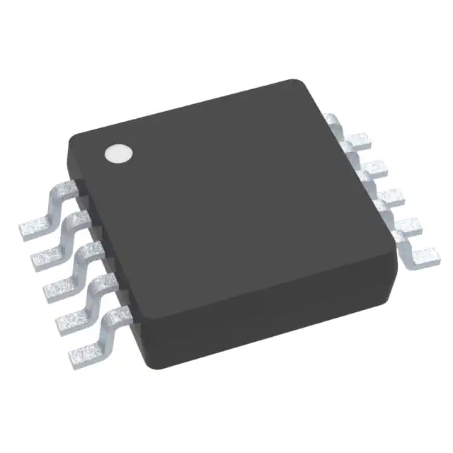
Analog Devices Inc. LTC2927IDDB#TRMPBF
- Part No.:
- LTC2927IDDB#TRMPBF
- Manufacturer:
- Analog Devices Inc.
- Category:
- Power Supply Controllers, Monitors
- Package:
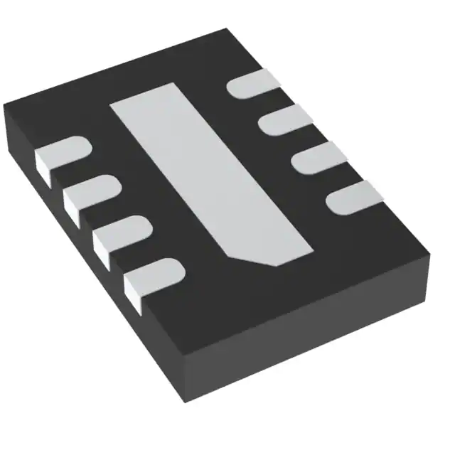
- 8-WFDFN Exposed Pad
- Datasheet:
-
 LTC2927IDDB#TRMPBF.pdf
- Description:
- IC POWER SUPPLY CONTROLLER 8DFN
- Quantity:
- Payment:

- Shipping:

Inventory:2,893
Please send an inquiry. Send us your inquiry, and we will respond immediately.
Product details
Overview
LTC2927IDDB#TRMPBF from Analog Devices (formerly Linear Technology) is a single-channel power supply tracking and sequencing controller IC designed for precise ramp-up/ramp-down coordination between master and slave DC/DC supplies. It delivers adjustable ramp rates (e.g., 100 V/s), ±5% current-mirror tracking accuracy, 0.8 V TRACK pin reference, and open-drain SDO shutdown output - enabling FPGA, microprocessor, and multi-rail point-of-load systems to meet strict voltage sequencing requirements during power-on and power-off.
For engineers reviewing the LTC2927IDDB#TRMPBF datasheet, LTC2927IDDB#TRMPBF pinout, LTC2927IDDB#TRMPBF application, or LTC2927IDDB#TRMPBF equivalent, this page provides verified functional context, validated pin-level circuit roles, confirmed tracking performance metrics, and real-world sequencing design constraints - all specific to the 8-lead DFN (3 mm × 2 mm) industrial-grade variant.
Technical Context
The LTC2927IDDB#TRMPBF implements an open-loop current-mirror tracking cell that servos the TRACK pin at 0.8 V and mirrors ITRACK to FB, enabling precise voltage ratio control without affecting slave supply stability or transient response. Its RAMP pin accepts either internal 10 µA pull-up/pull-down current (for capacitor-generated ramps) or external master signals.
RAMPBUF provides a low-impedance buffered version of RAMP (±2 mA drive capability) to drive resistive dividers connected to TRACK; ON pin controls ramp direction via 1.23 V threshold with 75 mV hysteresis; SDO asserts low until VCC > 2.5 V and ON > 1.23 V, coordinating slave supply enable timing.
Key Specifications
| Parameter | Value and Actual Design Meaning |
|---|---|
| Supply Voltage (VCC) | 2.9 V to 5.5 V - defines minimum operating headroom for reliable internal biasing and SDO assertion. |
| TRACK Pin Reference | 0.800 V (±30 mV) - sets servo point for current-mirror tracking; determines slave output voltage scaling via RTA/RTB resistor network. |
| RAMP Current Source/Sink | ±10 µA - sets master ramp rate when driving external CRAMP; enables 100 V/s ramp with 0.1 µF capacitor. |
| ON Pin Threshold | 1.230 V (±20 mV) with 75 mV hysteresis - controls ramp direction transition; supports resistive divider monitoring of input supply readiness. |
| FB Pin Clamp Voltage | 1.5 V to 2.3 V - prevents overdrive of slave DC/DC feedback node; ensures safe operation even under fault conditions. |
| Operating Temperature | –40°C to +85°C - qualified for industrial environments; matches LTC2927I grade specification. |
| Package | 8-lead (3 mm × 2 mm) plastic DFN - compact footprint optimized for point-of-load placement near sensitive FB nodes. |
Pinout & Package
Package: 8-lead (3 mm × 2 mm) plastic DFN (DDB), exposed pad (Pin 9) optional GND connection. Thermal resistance θJA = 76°C/W.
| Pin/Terminal | Circuit Role | Design Meaning |
|---|---|---|
| VCC (Pin 1) | Supply Input | Power rail for internal circuitry; requires 0.1 µF bypass to GND; UVLO activates SDO below 2.5 V. |
| SDO (Pin 2) | Open-Drain Shutdown Output | Drives slave RUN/SS low until VCC > 2.5 V and ON > 1.23 V; sinks ≥1 mA for compatible DC/DC enable inputs. |
| FB (Pin 3) | Feedback Control Output | Mirrors TRACK current to slave DC/DC feedback node; clamped at 2.3 V max to prevent overregulation. |
| GND (Pin 4) | Ground Reference | Primary signal and power return; exposed pad (Pin 9) may be tied to PCB GND for improved thermal performance. |
| TRACK (Pin 5) | Tracking Control Input | Servos at 0.8 V; sources up to 1 mA at VCC = 2.9 V; drives RAMPBUF-to-TRACK divider to set slave output profile. |
| RAMPBUF (Pin 6) | Ramp Buffer Output | Low-impedance replica of RAMP; drives RTA/RTB network; capable of ±2 mA output for robust divider drive. |
| RAMP (Pin 7) | Ramp Signal Input | Accepts internal ±10 µA current or external master ramp; grounded when unused to disable internal ramp generation. |
| ON (Pin 8) | Direction Control Input | 1.23 V threshold selects ramp-up (pull-up) or ramp-down (pull-down); supports supply-monitoring via resistive divider. |
Key Features
| Feature | Design Value |
|---|---|
| Open-loop tracking architecture | Eliminates pass element losses and preserves slave supply transient response and loop stability. |
| Adjustable ramp rate control | Set via external capacitor on RAMP pin (e.g., 0.1 µF → 100 V/s) or driven by external master supply. |
| Programmable tracking profiles | Supports coincident, offset, ratiometric, and sequenced ramping using only two external resistors per slave supply. |
| Integrated shutdown coordination | SDO output synchronizes slave supply enable with VCC and ON pin readiness - no external logic required. |
| High-impedance post-sequence state | FB and TRACK present negligible load after ramp completion, removing controller influence from final regulation. |
Applications
| VCORE and VI/O Supply Tracking | Microprocessor Power Sequencing |
|---|---|
Use Scenario: Coordinating 1.8 V I/O and 1.2 V core rails in an FPGA to prevent latch-up during power-up. IC Role / Device Role / Timing Role: LTC2927IDDB#TRMPBF acts as master-controlled tracking controller, generating synchronized ramp signals for both rails using shared RAMPBUF and independent TRACK networks. Use Value: Ensures |VI/O – VCORE| ≤ 0.6 V throughout ramp-up/down, meeting Xilinx Spartan-7 absolute maximum rating requirements. |
Use Scenario: Enabling 3.3 V system clock before releasing 1.2 V processor core and 2.5 V memory rails. IC Role / Device Role / Timing Role: LTC2927IDDB#TRMPBF configures sequential delays via RTA resistor networks to stagger slave supply activation timing. Use Value: Guarantees clock domain stability prior to core initialization, eliminating boot failures in ARM Cortex-M7-based industrial controllers. |
| Multiple Supply Systems | Point-of-Load Supplies |
Use Scenario: Managing four independent DC/DC outputs (1.0 V, 1.8 V, 2.5 V, 3.3 V) in a telecom line card with mixed ASIC/FPGA loads. IC Role / Device Role / Timing Role: LTC2927IDDB#TRMPBF serves as central tracking coordinator, using one device per critical rail to enforce inter-supply voltage offsets. Use Value: Enables compliance with IEEE 802.3af PoE+ sequencing mandates while minimizing board-level component count. |
Use Scenario: Fine-grained voltage ramp control directly adjacent to high-speed ADC/DAC power pins on a data acquisition module. IC Role / Device Role / Timing Role: LTC2927IDDB#TRMPBF mounts in 3 mm × 2 mm DFN package within 5 mm of slave DC/DC FB node to minimize noise-sensitive trace length. Use Value: Reduces FB node EMI susceptibility by >20 dB compared to remote tracking solutions, preserving 16-bit ENOB performance. |
Equivalent & Alternatives
The following parts are listed as comparable options for similar power supply tracking applications.
| Alternative Part | Technical Difference | Application Difference | Selection Advice |
|---|---|---|---|
| LTC2928IDDB#TRMPBF | Dual-channel version with identical per-channel specs; shares same DFN package and pinout except for duplicated SDO/FB/ON pins. | Replaces two LTC2927 devices in dual-rail systems; eliminates inter-device matching variance but increases layout complexity. | Select when coordinating two independent slave supplies from one master ramp - reduces BOM count vs. dual LTC2927 implementation. |
| TPS6508641RSLR | Integrated PMIC with fixed 4-rail sequencing, non-adjustable ramp rates, and embedded LDOs; no external RAMP capacitor support. | Targets pre-defined SoC power trees (e.g., TI AM62x); lacks flexibility for custom ramp profiles or third-party DC/DC controllers. | Choose for cost-sensitive, high-volume SoC designs where sequencing is static and ramp tuning is unnecessary. |
Compared with LTC2928IDDB#TRMPBF and TPS6508641RSLR, the LTC2927IDDB#TRMPBF offers unmatched analog programmability for arbitrary ramp shapes and voltage offsets using passive components, while maintaining minimal footprint and zero impact on slave supply dynamics - making it optimal for flexible, high-reliability industrial and test equipment designs.
Availability
LTC2927IDDB#TRMPBF is available at Aetrix Electronics and suitable for FPGA power management, microprocessor sequencing, and multi-rail industrial power systems requiring stable component supply across extended temperature ranges and long production lifecycles.
Supply support for LTC2927IDDB#TRMPBF includes scheduled delivery planning, volume procurement assistance, BOM continuity management, traceable sourcing, and lifecycle availability coordination for OEM customers, industrial embedded developers, connected-device designers, and electronics production programs.
Manufacturer
Analog Devices, Inc. (acquired Linear Technology in 2017) is a global leader in high-performance analog, mixed-signal, and digital signal processing semiconductors for precision instrumentation, industrial automation, and communications infrastructure.
The LTC2927 belongs to Linear's Power Management portfolio, specifically engineered for analog-controlled power supply coordination in systems where digital sequencing ICs lack sufficient flexibility or introduce unacceptable latency in feedback-critical paths.
FAQ
What is the primary function of the LTC2927IDDB#TRMPBF in a power system?
The LTC2927IDDB#TRMPBF is a precision analog tracking controller that coordinates voltage ramp-up and ramp-down sequences between master and slave DC/DC supplies. It uses an open-loop current mirror to force the slave supply's output to follow a defined profile - such as coincident, offset, ratiometric, or delayed - without inserting series loss elements or degrading the slave supply's transient response. This makes LTC2927IDDB#TRMPBF ideal for FPGA, ASIC, and microprocessor applications with strict inter-rail voltage margin requirements.
How does the LTC2927IDDB#TRMPBF achieve tracking without affecting slave supply stability?
The LTC2927IDDB#TRMPBF achieves tracking via open-loop current mirroring: it sources/sinks current at the TRACK pin (servoing at 0.8 V) and mirrors that current to the FB pin, thereby adjusting the slave DC/DC's feedback node. Because no series pass element is inserted and no closed-loop error amplifier interacts with the slave's control loop, the LTC2927IDDB#TRMPBF introduces no phase shift or gain perturbation. Verified in application circuits, this preserves the original DC/DC converter's bandwidth, phase margin, and load-step response - a key advantage over op-amp-based tracking solutions.
Can the LTC2927IDDB#TRMPBF support both ramp-up and ramp-down tracking?
Yes, the LTC2927IDDB#TRMPBF supports bidirectional tracking through its ON pin: when ON rises above 1.23 V, a 10 µA pull-up current charges the external RAMP capacitor, generating an upward ramp; when ON falls below ~1.225 V (1.23 V minus 75 mV hysteresis), a 10 µA pull-down current discharges the same capacitor, producing a symmetric downward ramp. This allows matched slew rates for both power-on and power-off transitions - critical for hot-swap and graceful shutdown in telecom and server applications using LTC2927IDDB#TRMPBF.
What is the role of the SDO pin on the LTC2927IDDB#TRMPBF?
The SDO pin on the LTC2927IDDB#TRMPBF is an open-drain output used to coordinate slave supply enable timing. It remains low until both VCC exceeds 2.5 V (UVLO release) and the ON pin exceeds 1.23 V, ensuring the slave DC/DC only starts regulating after the tracking controller is fully powered and armed. SDO pulls low again when both ON < 1.23 V and RAMP < 200 mV, supporting controlled shutdown. This eliminates need for external power-good logic and simplifies sequencing in multi-rail systems built around LTC2927IDDB#TRMPBF.
Is the LTC2927IDDB#TRMPBF compatible with DC/DC converters having different feedback reference voltages?
Yes, the LTC2927IDDB#TRMPBF supports DC/DC converters with varying FB reference voltages (e.g., 0.6 V, 0.8 V, 1.235 V) through its resistor-based TRACK network. The relationship VOUT = VTRACK × (1 + RFA/RFB) × (RTB/RTA) allows full scaling independence. For example, a 1.235 V FB converter and a 0.8 V FB converter can both be tracked from the same LTC2927IDDB#TRMPBF RAMPBUF output by selecting appropriate RTA/RTB ratios - confirmed in Figures 9–16 of the official datasheet for LTC2927IDDB#TRMPBF.
LTC2927IDDB#TRMPBF Specifications
- Product attributes
- Attribute value
- Manufacturer:
- Analog Devices Inc.
- Series:
- -
- Package/Case:
- 8-WFDFN Exposed Pad
- Packaging:
- Tape & Reel (TR)
- Product Status:
- Active
- Programmable:
- Not Verified
- Applications:
- Power Supply Controller
- Voltage - Input:
- -
- Voltage - Supply:
- 2.9V ~ 5.5V
- Current - Supply:
- 560 µA
- Operating Temperature:
- -40°C ~ 85°C
- Grade:
- -
- Qualification:
- -
- Mounting Type:
- Surface Mount
- Supplier Device Package:
- 8-DFN (3x2)
LTC2927IDDB#TRMPBF FAQ
1.How can I place an order for LTC2927IDDB#TRMPBF through Aetrix?
Please submit a Request for Quotation (RFQ) for LTC2927IDDB#TRMPBF on Aetrix. Our sales agent will provide a competitive quotation and guide you through the order confirmation once you accept the terms.
2.Are the price and stock information for LTC2927IDDB#TRMPBF reliable?
The price and inventory of LTC2927IDDB#TRMPBF are updated periodically and may fluctuate due to market conditions. Stock and pricing data are typically refreshed every 24 hours. Quotation validity for LTC2927IDDB#TRMPBF is usually 5 days.
3.What payment methods are accepted for LTC2927IDDB#TRMPBF?
We accept Wire Transfer, PayPal, Credit Card, Western Union, MoneyGram, and Escrow for LTC2927IDDB#TRMPBF transactions.
Note: Certain payment methods may incur a processing fee.
4.How is shipping managed for LTC2927IDDB#TRMPBF?
LTC2927IDDB#TRMPBF orders can be shipped via leading logistics carriers, including DHL, UPS, FedEx, TNT, or Registered Mail.
Once your LTC2927IDDB#TRMPBF order is processed, you will receive an email with the shipment details and tracking number.
Note: Tracking information may take up to 24 hours to appear. Express delivery typically takes 3–5 business days.
5.How can I obtain technical support or documentation for LTC2927IDDB#TRMPBF?
For technical support, including LTC2927IDDB#TRMPBF datasheets, pinout diagrams, or application guidance, please contact our engineering support team. They can provide detailed documentation and assistance for your LTC2927IDDB#TRMPBF requirements.
6.How does Aetrix verify that LTC2927IDDB#TRMPBF is sourced from the original manufacturer or authorized distributors?
All LTC2927IDDB#TRMPBF products on Aetrix are procured from qualified distributors and authorized channels. Our dedicated quality assurance team conducts strict verification, including traceability checks and, if necessary, third-party testing. This ensures that LTC2927IDDB#TRMPBF meets industry standards.
7.What is the process for return or replacement of LTC2927IDDB#TRMPBF?
All LTC2927IDDB#TRMPBF units undergo pre-shipment inspection (PSI). If there is an issue with LTC2927IDDB#TRMPBF, returns or replacements are accepted under the following conditions:
1.Quantity discrepancies, incorrect items, or visible external defects (such as breakage or corrosion), acknowledged by Aetrix.
2.The issue is reported within 90 days of delivery.
3.The LTC2927IDDB#TRMPBF part is unused and in its original packaging.
Return procedure for LTC2927IDDB#TRMPBF:
1.Submit a request within 90 days.
2.Obtain a Return Material Authorization (RMA) from Aetrix.
LTC2927IDDB#TRMPBF Tags

-
UC3845AD8TR
Texas Instruments
-
UC2843AD8TR
Texas Instruments

-
LM3880MFX-1AE/NOPB
Texas Instruments
-
LM3880MFX-1AA/NOPB
Texas Instruments
-
INA234AIYBJR
Texas Instruments

-
INA700AYWFR
Texas Instruments
-
LM3880MF-1AE/NOPB
Texas Instruments
-
LM3880MF-1AA/NOPB
Texas Instruments
-
LM3881MM/NOPB
Texas Instruments
-
UCC2802DTR
Texas Instruments
-
NCP4305DMTTWG
onsemi
-
INA237AIDGSR
Texas Instruments
Tech Hub

A practical engineering guide to 3.3V and 5V logic compatibility, input thresholds, resistor dividers, translator ICs, MOSFET level shifting, I2C pull-ups, timing limits and power-sequencing risks.

The 74HC595 uses push-pull logic outputs, while the TPIC6B595 uses 50 V open-drain DMOS sinks for higher-power loads. This guide compares timing, current limits, 3.3 V interfacing, load wiring, thermal…

The 74HC595 converts serial data into eight stable parallel outputs. This guide covers pin functions, shift and storage timing, OE and MR behavior, drive-current limits, cascading, voltage compatibilit…

A technical comparison of level-sensitive latches and edge-triggered flip-flops, covering timing windows, setup and hold limits, master–slave operation, time borrowing, race-through, HDL inference and…

A D latch stores one bit while Enable controls when data can pass. This reference covers gate-level operation, truth tables, transparency, setup and hold timing, LE versus OE, common ICs and practical …

An SR latch stores one bit through cross-coupled feedback. This engineering reference covers NOR and NAND implementations, truth tables, forbidden-state recovery, gated operation, switch debouncing, fa…

Latch circuits retain one bit through feedback. This technical reference covers SR and D latches, truth tables, transparency, timing limits, latch-versus-flip-flop behavior, applications and common log…

An engineering guide to LED driver operation, constant-current and constant-voltage outputs, linear and switching topologies, dimming, IC selection, calculations, replacement compatibility, and fault c…

Operational amplifier guide covering op amp basics, feedback, ideal vs real op amps, common configurations, buffer circuits, offset, bias current, gain-bandwidth, slew rate, rail-to-rail limits and sel…

Jumper cables guide covering safe connection order, red and black clamp placement, final ground connection, cable gauge, length, clamp quality, copper vs CCA cables, jump starter comparison and battery…


