
 My Inquiry
 My Account


Analog Devices Inc. LTC2956CMS-1#PBF
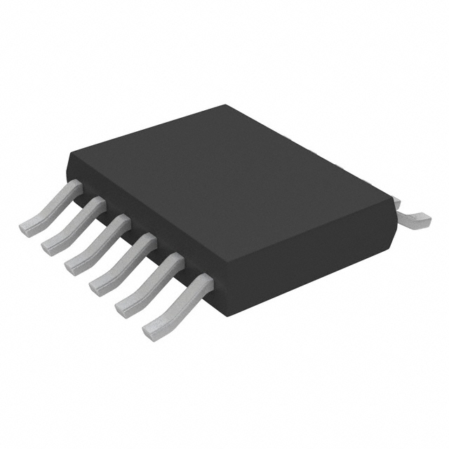
- Part No.:
- LTC2956CMS-1#PBF
- Manufacturer:
- Analog Devices Inc.
- Category:
- Power Supply Controllers, Monitors
- Package:
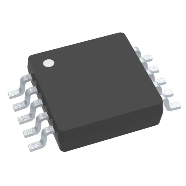
- 12-TSSOP (0.118", 3.00mm Width)
- Datasheet:
-
 LTC2956CMS-1#PBF.pdf
- Description:
- IC PB ON/OFF CONTROLLER 12MSOP
- Quantity:
- Payment:

- Shipping:

Inventory:181
Please send an inquiry. Send us your inquiry, and we will respond immediately.
Product details
Overview
LTC2956CMS-1#PBF from Analog Devices (formerly Linear Technology) is a micropower wake-up timer IC with pushbutton control and active-high enable output, designed for periodic power cycling of battery-powered systems. It operates from 1.5V to 36V, delivers 0.8µA quiescent current in awake state and 0.3µA in shutdown, and supports configurable wake-up periods from 250ms to 39 days - enabling use in remote sensor nodes performing temperature monitoring or image capture.
For engineers reviewing the LTC2956CMS-1#PBF datasheet, LTC2956CMS-1#PBF pinout, LTC2956CMS-1#PBF application, or LTC2956CMS-1#PBF equivalent, key selection criteria include its MSOP-12 package, -1 variant's low-leakage EN output for direct DC/DC converter control, adjustable ONMAX timing capacitor interface, and ±25kV HBM ESD protection on PB input.
Technical Context
The LTC2956CMS-1#PBF implements a dual-timer architecture: a digitally controlled wake-up period timer (250ms–39 days) set via PERIOD and RANGE resistors, and an analog-digital hybrid maximum awake timer (tONMAX) set by an external capacitor on ONMAX. Its internal 2kHz oscillator feeds a programmable divider (÷1 to ÷2²²) for precise long-interval timing.
It features three status outputs (ONALERT, OFFALERT, PBOUT), debounced pushbutton logic with 32ms typical debounce time, and configurable power-up mode (RUN or SHUTDOWN) determined by the LONG pin voltage divider. The -1 variant provides an active-high EN output with 900kΩ internal pull-up and 0.4V max VOL at 1mA, optimized for driving regulator RUN pins.
Key Specifications
| Parameter | Value and Actual Design Meaning |
|---|---|
| Supply Voltage Range | 1.5V to 36V - supports single-cell Li-ion up to 24V industrial rails without external regulation. |
| Quiescent Current (Awake) | 0.8µA typical - enables multi-year operation on coin cells in periodic sensing applications. |
| Shutdown Current | 0.3µA typical - minimizes battery drain during storage or transport mode. |
| Wake-Up Period Range | 250ms to 39 days - selectable via resistor network on PERIOD/RANGE pins for flexible duty-cycle tuning. |
| Maximum Awake Time Control | Capacitor-programmable (13.3ms/nF) on ONMAX pin - sets hard upper bound on system-on duration to prevent excessive battery discharge. |
| Pushbutton Debounce | 32ms typical - eliminates mechanical switch chatter without requiring external RC filtering. |
| ESD Protection (PB) | ±25kV HBM - ensures robustness in handheld or field-deployed equipment with exposed buttons. |
| Operating Temperature | 0°C to 70°C - qualified for commercial-grade embedded systems and portable instrumentation. |
Pinout & Package
Package: 12-Lead Plastic MSOP (3mm × 4.4mm), exposed pad not connected (non-thermal).
| Pin/Terminal | Circuit Role | Design Meaning |
|---|---|---|
| VIN | Power supply input | Accepts 1.5V–36V unregulated input; includes 1.24V UVLO with 100mV hysteresis. |
| GND | Device ground reference | Common return for all analog and digital circuitry; no exposed pad connection required in MSOP. |
| EN | Active-high enable output | Drives RUN/SHDN pin of DC/DC converters; 0.4V max VOL at 1mA, internal 900kΩ pull-up to VCC. |
| PB | Pushbutton input | Active-low with 900kΩ internal pull-up to 3.3V regulator; ±25kV HBM rated; threshold 0.9V typical. |
| SLEEP | System sleep request input | Falling edge triggers immediate transition to Sleep state; held high >tLONG forces Shutdown mode. |
| ONMAX | Maximum awake time capacitor input | Connects to GND via capacitor (13.3ms/nF); floating = 8ms min awake time; tied to GND disables timer. |
| PERIOD | Wake-up interval resistor input | Resistor to GND sets base timing; combined with RANGE resistor to select 250ms–39 day range. |
| RANGE | Timing range selection input | Resistor to GND + 100kΩ to LONG selects decade-scale multiplier for PERIOD resistor value. |
| LONG | Long-press timeout configuration | Resistor to GND sets tLONG (128ms–16.4s); determines SLEEP/PB hold time to enter Shutdown mode. |
| ONALERT | Open-drain on-alert output | Pulled low during first Awake state after power-up or exit from Shutdown - signals boot initialization need. |
| OFFALERT | Open-drain off-alert output | Pulled low for 1s (tOFF) during Shutting Off state - alerts system to perform graceful shutdown tasks. |
| PBOUT | Debounced pushbutton open-drain output | Reflects cleaned PB signal; first pulse ≥128ms wide for reliable MCU interrupt detection post-power-on. |
Key Features
| Feature | Design Value |
|---|---|
| Configurable wake-up period | 250ms to 39 days via two external resistors - eliminates firmware dependency for timing changes. |
| Capacitor-programmed maximum awake time | tONMAX = 13.3ms/nF on ONMAX pin - prevents runaway system-on events due to firmware lockup. |
| Active-high EN output (-1 variant) | Low-leakage (≤100nA) drive with 0.4V VOL at 1mA - directly interfaces with common DC/DC RUN pins. |
| Three status alert outputs | ONALERT, OFFALERT, PBOUT provide hardware-level event signaling without MCU polling overhead. |
| Programmable power-up mode | Set via LONG pin voltage divider - enables factory-default SHUTDOWN for shipped devices with installed batteries. |
| Integrated pushbutton debounce | 32ms hardware debounce with echo output (PBOUT) - removes need for external RC or firmware filtering. |
Applications
| Remote Environmental Sensor Node | Portable Medical Data Logger |
|---|---|
|
Use Scenario: Battery-powered outdoor node measuring temperature/humidity every 2 hours and transmitting via LoRaWAN. IC Role / Device Role / Timing Role: LTC2956CMS-1#PBF controls power to MCU, sensor, and radio; wakes system only for measurement/transmission burst. Use Value: Extends CR2032 battery life from weeks to >2 years by reducing average current to sub-µA level. |
Use Scenario: Handheld device recording ECG data at scheduled intervals, stored locally until USB upload. IC Role / Device Role / Timing Role: LTC2956CMS-1#PBF gates power to analog front-end and microcontroller; ONALERT triggers boot initialization. Use Value: Guarantees consistent 8ms minimum awake time for ADC calibration and memory initialization before sampling. |
| Industrial Intervalometer for Predictive Maintenance | Smart Asset Tracker (GPS + Cellular) |
|
Use Scenario: Ruggedized enclosure monitoring vibration on rotating machinery every 15 minutes using MEMS accelerometer. IC Role / Device Role / Timing Role: LTC2956CMS-1#PBF drives P-channel MOSFET via EN to power entire subsystem; OFFALERT signals 1s pre-shutdown window. Use Value: Prevents data corruption during flash write by ensuring MCU completes logging before power removal. |
Use Scenario: Solar-charged tracker reporting location every 6 hours; enters deep sleep between transmissions. IC Role / Device Role / Timing Role: LTC2956CMS-1#PBF manages power sequencing: ONALERT wakes MCU, PBOUT handles button-press menu navigation. Use Value: Enables reliable button interaction with 128ms initial PBOUT pulse - sufficient for slow-starting GPS modules. |
Equivalent & Alternatives
The following parts are listed as comparable options for similar wake-up timer applications.
| Alternative Part | Technical Difference | Application Difference | Selection Advice |
|---|---|---|---|
| LTC2956CMS-2#PBF | Active-low EN output drives P-channel MOSFET gate directly; higher VOL (VIN – 1.5V) vs. -1's fixed 1.5V VOH. | Suitable where system requires high-side PMOS switching instead of regulator RUN control. | Select -2 when driving external high-side FET; -1 preferred for direct DC/DC enable interfacing. |
| TPS3897A33DBVR | Fixed 3.3V supply monitor with manual reset and watchdog; no programmable wake-up timer or ONMAX capacitor interface. | Limited to power-fail detection and basic reset - lacks periodic wake capability or adjustable timing. | Choose TPS3897 only for simple supply supervision; LTC2956CMS-1#PBF required for autonomous timed wake-up. |
Compared with LTC2956CMS-2#PBF, the LTC2956CMS-1#PBF offers lower EN output leakage and simpler regulator interface, while TPS3897A33DBVR lacks wake-up functionality entirely - making LTC2956CMS-1#PBF the sole option for battery-efficient periodic task execution.
Availability
LTC2956CMS-1#PBF is available at Aetrix Electronics and suitable for remote environmental sensing, portable medical data logging, and industrial predictive maintenance applications requiring stable component supply across multi-year production cycles.
Supply support for LTC2956CMS-1#PBF includes scheduled delivery planning, volume procurement assistance, BOM continuity management, traceable sourcing, and lifecycle availability coordination for OEM customers, industrial embedded developers, connected-device designers, and electronics production programs.
Manufacturer
Analog Devices acquired Linear Technology in 2017 and maintains its precision analog and power management portfolio with rigorous automotive and industrial qualification standards.
The LTC2956 product line delivers ultra-low-power, resistor/capacitor-configurable wake-up timers for battery-critical applications - emphasizing long-term reliability, wide input voltage tolerance, and hardware-based timing autonomy.
FAQ
What is the function of the ONMAX pin on the LTC2956CMS-1#PBF?
The ONMAX pin on the LTC2956CMS-1#PBF accepts an external capacitor to set the maximum allowed awake time (tONMAX) at 13.3ms per nanofarad. When the capacitor is connected to GND, the LTC2956CMS-1#PBF enforces this upper bound on system-on duration - preventing excessive battery drain if firmware hangs. If left floating, tONMAX defaults to 8ms; tying it to GND disables the timer entirely.
How does the LTC2956CMS-1#PBF differ from the LTC2956CMS-2#PBF?
The LTC2956CMS-1#PBF features an active-high EN output optimized for driving DC/DC converter RUN pins, while the LTC2956CMS-2#PBF provides an active-low EN output capable of directly controlling a P-channel MOSFET gate. Both share identical timing, debounce, and alert functions, but their EN polarity and drive characteristics target different power architecture topologies - making them non-interchangeable without board-level redesign.
Can the LTC2956CMS-1#PBF be used with a 1.8V supply?
Yes, the LTC2956CMS-1#PBF operates down to 1.5V, so it functions reliably at 1.8V. All specifications - including 0.8µA quiescent current, 0.9V PB threshold, and 0.4V EN VOL - are guaranteed over the full 1.5V–36V range. No derating or external biasing is required at 1.8V, making it suitable for single-cell LiFePO₄ or alkaline-powered designs.
What is the purpose of the OFFALERT pin on the LTC2956CMS-1#PBF?
The OFFALERT pin on the LTC2956CMS-1#PBF is an open-drain output pulled low for exactly 1 second (tOFF) whenever the device transitions from RUN mode to SHUTDOWN mode. This provides a hardware-level warning that system power will be removed shortly - allowing the MCU to complete flash writes, save registers, or trigger safe state entry before EN goes inactive.
How is the wake-up period configured on the LTC2956CMS-1#PBF?
The wake-up period on the LTC2956CMS-1#PBF is set using two external resistors: one from PERIOD to GND (RPERIOD = 32.4kΩ–324kΩ) and another from RANGE to GND (RRANGE), with a fixed 100kΩ resistor between RANGE and LONG. This resistor network selects both the base timing interval and its decade-scale multiplier - enabling precise adjustment from 250ms to 39 days without firmware or crystal dependencies.
LTC2956CMS-1#PBF Specifications
- Product attributes
- Attribute value
- Manufacturer:
- Analog Devices Inc.
- Series:
- -
- Package/Case:
- 12-TSSOP (0.118", 3.00mm Width)
- Packaging:
- Tube
- Product Status:
- Active
- Programmable:
- Not Verified
- Applications:
- Wake Up Timer
- Voltage - Input:
- -
- Voltage - Supply:
- 1.5V ~ 36V
- Current - Supply:
- 3 µA
- Operating Temperature:
- 0°C ~ 70°C
- Grade:
- -
- Qualification:
- -
- Mounting Type:
- Surface Mount
- Supplier Device Package:
- 12-MSOP
LTC2956CMS-1#PBF FAQ
1.How can I place an order for LTC2956CMS-1#PBF through Aetrix?
Please submit a Request for Quotation (RFQ) for LTC2956CMS-1#PBF on Aetrix. Our sales agent will provide a competitive quotation and guide you through the order confirmation once you accept the terms.
2.Are the price and stock information for LTC2956CMS-1#PBF reliable?
The price and inventory of LTC2956CMS-1#PBF are updated periodically and may fluctuate due to market conditions. Stock and pricing data are typically refreshed every 24 hours. Quotation validity for LTC2956CMS-1#PBF is usually 5 days.
3.What payment methods are accepted for LTC2956CMS-1#PBF?
We accept Wire Transfer, PayPal, Credit Card, Western Union, MoneyGram, and Escrow for LTC2956CMS-1#PBF transactions.
Note: Certain payment methods may incur a processing fee.
4.How is shipping managed for LTC2956CMS-1#PBF?
LTC2956CMS-1#PBF orders can be shipped via leading logistics carriers, including DHL, UPS, FedEx, TNT, or Registered Mail.
Once your LTC2956CMS-1#PBF order is processed, you will receive an email with the shipment details and tracking number.
Note: Tracking information may take up to 24 hours to appear. Express delivery typically takes 3–5 business days.
5.How can I obtain technical support or documentation for LTC2956CMS-1#PBF?
For technical support, including LTC2956CMS-1#PBF datasheets, pinout diagrams, or application guidance, please contact our engineering support team. They can provide detailed documentation and assistance for your LTC2956CMS-1#PBF requirements.
6.How does Aetrix verify that LTC2956CMS-1#PBF is sourced from the original manufacturer or authorized distributors?
All LTC2956CMS-1#PBF products on Aetrix are procured from qualified distributors and authorized channels. Our dedicated quality assurance team conducts strict verification, including traceability checks and, if necessary, third-party testing. This ensures that LTC2956CMS-1#PBF meets industry standards.
7.What is the process for return or replacement of LTC2956CMS-1#PBF?
All LTC2956CMS-1#PBF units undergo pre-shipment inspection (PSI). If there is an issue with LTC2956CMS-1#PBF, returns or replacements are accepted under the following conditions:
1.Quantity discrepancies, incorrect items, or visible external defects (such as breakage or corrosion), acknowledged by Aetrix.
2.The issue is reported within 90 days of delivery.
3.The LTC2956CMS-1#PBF part is unused and in its original packaging.
Return procedure for LTC2956CMS-1#PBF:
1.Submit a request within 90 days.
2.Obtain a Return Material Authorization (RMA) from Aetrix.
LTC2956CMS-1#PBF Tags

-
UC3845AD8TR
Texas Instruments
-
UC2843AD8TR
Texas Instruments

-
LM3880MFX-1AE/NOPB
Texas Instruments
-
LM3880MFX-1AA/NOPB
Texas Instruments
-
INA234AIYBJR
Texas Instruments

-
INA700AYWFR
Texas Instruments
-
LM3880MF-1AE/NOPB
Texas Instruments
-
LM3880MF-1AA/NOPB
Texas Instruments
-
LM3881MM/NOPB
Texas Instruments
-
UCC2802DTR
Texas Instruments
-
NCP4305DMTTWG
onsemi
-
INA237AIDGSR
Texas Instruments
Tech Hub

A practical engineering guide to 3.3V and 5V logic compatibility, input thresholds, resistor dividers, translator ICs, MOSFET level shifting, I2C pull-ups, timing limits and power-sequencing risks.

The 74HC595 uses push-pull logic outputs, while the TPIC6B595 uses 50 V open-drain DMOS sinks for higher-power loads. This guide compares timing, current limits, 3.3 V interfacing, load wiring, thermal…

The 74HC595 converts serial data into eight stable parallel outputs. This guide covers pin functions, shift and storage timing, OE and MR behavior, drive-current limits, cascading, voltage compatibilit…

A technical comparison of level-sensitive latches and edge-triggered flip-flops, covering timing windows, setup and hold limits, master–slave operation, time borrowing, race-through, HDL inference and…

A D latch stores one bit while Enable controls when data can pass. This reference covers gate-level operation, truth tables, transparency, setup and hold timing, LE versus OE, common ICs and practical …

An SR latch stores one bit through cross-coupled feedback. This engineering reference covers NOR and NAND implementations, truth tables, forbidden-state recovery, gated operation, switch debouncing, fa…

Latch circuits retain one bit through feedback. This technical reference covers SR and D latches, truth tables, transparency, timing limits, latch-versus-flip-flop behavior, applications and common log…

An engineering guide to LED driver operation, constant-current and constant-voltage outputs, linear and switching topologies, dimming, IC selection, calculations, replacement compatibility, and fault c…

Operational amplifier guide covering op amp basics, feedback, ideal vs real op amps, common configurations, buffer circuits, offset, bias current, gain-bandwidth, slew rate, rail-to-rail limits and sel…

Jumper cables guide covering safe connection order, red and black clamp placement, final ground connection, cable gauge, length, clamp quality, copper vs CCA cables, jump starter comparison and battery…


