
 My Inquiry
 My Account


Analog Devices Inc. LTC4070EMS8E#TRPBF
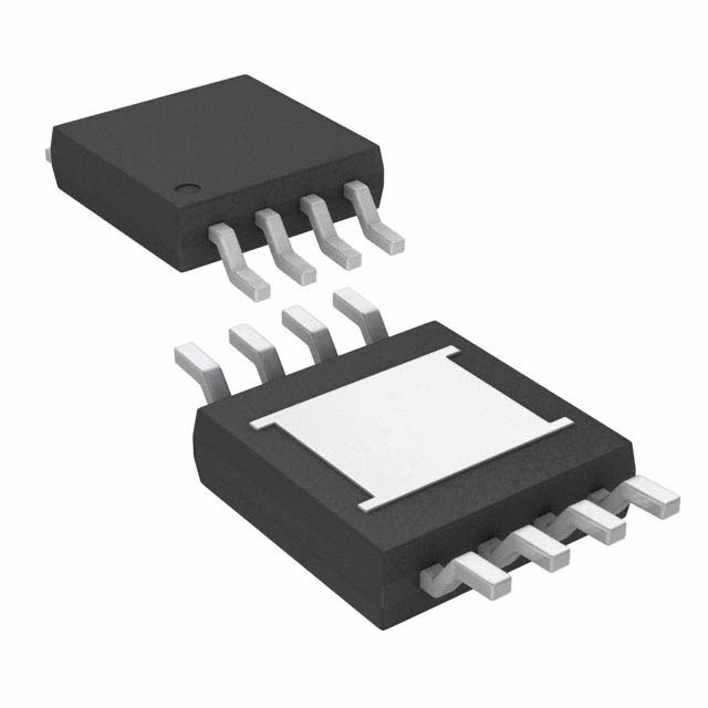
- Part No.:
- LTC4070EMS8E#TRPBF
- Manufacturer:
- Analog Devices Inc.
- Category:
- Battery Chargers
- Package:
- 8-TSSOP, 8-MSOP (0.118", 3.00mm Width) Exposed Pad
- Datasheet:
-
 LTC4070EMS8E#TRPBF.pdf
- Description:
- IC BATT CHG LI-ION 8MSOP
- Quantity:
- Payment:

- Shipping:

Inventory:3,425
Please send an inquiry. Send us your inquiry, and we will respond immediately.
Product details
Overview
LTC4070EMS8E#TRPBF from Analog Devices is a Li-ion/polymer shunt battery charger IC with 450nA quiescent current, ±1% float voltage accuracy (4.0V/4.1V/4.2V pin-selectable), and integrated NTC-based thermal qualification for battery protection. It delivers up to 50mA internal shunt current and supports external PFET boosting to 500mA, enabling energy harvesting, solar backup, and thin-film battery charging in ultra-low-power systems.
For engineers reviewing the LTC4070EMS8E#TRPBF datasheet, LTC4070EMS8E#TRPBF pinout, LTC4070EMS8E#TRPBF application, or LTC4070EMS8E#TRPBF equivalent, this page provides verified pin functions, NTC-qualified float voltage behavior, shunt current limits, thermal derating data, and real-world design constraints for intermittent low-current sources like photovoltaic cells and ambient energy harvesters.
Technical Context
The LTC4070EMS8E#TRPBF implements a precision shunt regulation architecture where charge current is determined by an external resistor (RIN) and regulated via dynamic current sinking into VCC. Its 3-state ADJ pin decodes GND/floating/VCC to select 4.0V/4.1V/4.2V base float voltage with ±1% tolerance across –40°C to 125°C.
NTC qualification operates via pulsed 0.002% duty-cycle biasing of NTCBIAS, comparing NTC voltage against four internal resistive taps (36.5%, 29.0%, 22.8%, 17.8%) to trigger fixed-step float voltage reduction (50mV/75mV/100mV per 10°C above 40°C) depending on ADJ state - ensuring battery safety without continuous power draw.
Key Specifications
| Parameter | Value and Actual Design Meaning |
|---|---|
| Float Voltage Options | 4.0V (ADJ = GND), 4.1V (ADJ = floating), 4.2V (ADJ = VCC); ±1% accuracy over full temperature and shunt current range |
| Max Internal Shunt Current | 50mA at VCC > VFLOAT; sets upper bound on RIN selection for thermal safety and regulation stability |
| Quiescent Operating Current | 450nA typical at VHBO low; enables multi-year operation on thin-film batteries during idle periods |
| NTC Float Voltage Step | 50mV/75mV/100mV per 10°C above 40°C (ADJ = GND/floating/VCC); ensures predictable thermal derating without software |
| HBO Threshold Accuracy | VHBTH = 15–60mV below effective float voltage; defines precise high-battery detection window for system-level charge management |
| LBO Threshold | VLBTH = 3.08–3.34V falling; provides reliable low-voltage warning for backup power switchover or load disconnect |
| Package Thermal Resistance | θJA = 40°C/W (MS8E); junction rise ≈8°C at 50mA shunt, critical for PCB copper area and heatsinking decisions |
Pinout & Package
Package: 8-lead plastic MSOP (MS8E), 3mm × 3mm footprint, 0.75mm profile, exposed pad (Pin 9) must be soldered to PCB ground for rated thermal performance (θJA = 40°C/W).
| Pin/Terminal | Circuit Role | Design Meaning |
|---|---|---|
| NTCBIAS (Pin 1) | NTC bias reference output | Pulsed 0.002% duty-cycle voltage source; connects to top of NTC bias resistor; minimize parasitic capacitance |
| NTC (Pin 2) | NTC thermistor input | Compares against internal divider taps; grounds to thermistor; connect to VCC if unused |
| ADJ (Pin 3) | Float voltage programming input | 3-state logic: GND→4.0V, floating→4.1V, VCC→4.2V; sampled every 1.5s to reject board leakage |
| HBO (Pin 4) | High battery status output | CMOS high-active signal; asserts when VCC within VHBTH of VFLOAT_EFF; hysteresis = 100mV |
| GND (Pin 5) | Power and signal ground | Primary ground reference; exposed pad (Pin 9) must be connected to PCB ground plane |
| LBO (Pin 6) | Low battery status output | CMOS high-active signal; asserts when VCC < VLBTH (3.08–3.34V); hysteresis = 220–350mV |
| DRV (Pin 7) | External PFET gate drive | Sinks ≤3µA; drives gate of external P-channel MOSFET to boost shunt current beyond 50mA |
| VCC (Pin 8) | Input supply and battery node | Regulated shunt target node; sinks up to 50mA; requires ≥0.1µF decoupling if no battery present |
Key Features
| Feature | Design Value |
|---|---|
| Ultralow 450nA operating current | Enables direct integration with microwatt energy harvesters (e.g., indoor PV, thermal, RF) without draining storage |
| Pin-selectable 4.0V/4.1V/4.2V float voltage | Eliminates external DAC or resistor ladder; supports LiCoO₂, LiMn₂O₄, and LiFePO₄-compatible chemistries via hardware configuration |
| NTC-qualified float voltage stepping | Reduces float voltage in fixed 50/75/100mV steps per 10°C above 40°C - prevents thermal runaway without microcontroller intervention |
| Low/high battery status outputs (HBO/LBO) | Provides autonomous system-level monitoring: HBO signals near-full charge; LBO triggers backup load activation or shutdown |
| Thermally enhanced MSOP package | 40°C/W θJA allows sustained 50mA shunt operation with minimal PCB copper; exposed pad mandatory for spec compliance |
Applications
| Energy Harvesting Backup Power | Solar-Powered Remote Sensors |
|---|---|
|
Use Scenario: Indoor light-harvesting circuit powering wireless sensor node with thin-film Li-ion battery. IC Role / Device Role / Timing Role: Shunt regulator maintaining battery at 4.1V while drawing only 450nA when light source is absent. Use Value: Extends functional lifetime beyond 10 years by eliminating standby discharge path; NTC qualification prevents overheating in enclosed enclosures. |
Use Scenario: Outdoor environmental monitor using small PV panel to recharge Li-ion battery during daylight. IC Role / Device Role / Timing Role: Primary charge controller with pulsed NTCBIAS and ADJ = floating for 4.1V float; DRV drives external PFET under peak insolation. Use Value: Achieves <10nA battery discharge at night via HBO-triggered isolation transistor control; thermal step-down avoids battery degradation at summer temperatures. |
| Memory Backup in Industrial PLCs | Automotive Telematics Data Logger |
|
Use Scenario: SRAM retention during main power loss in programmable logic controller with supercapacitor-assisted hold-up. IC Role / Device Role / Timing Role: Low-quiescent shunt charger topping off backup Li-ion cell; LBO signals host MCU when voltage drops below 3.2V. Use Value: Guarantees >72-hour memory retention after AC failure; ±1% float accuracy prevents overvoltage stress on aging cells. |
Use Scenario: Crash-data logger powered by vehicle battery with secondary Li-ion backup for post-accident transmission. IC Role / Device Role / Timing Role: NTC-monitored shunt charger maintaining 4.2V float; HBO confirms readiness; thermal qualification disables charging above 70°C engine bay temps. Use Value: Meets AEC-Q100 Grade 1 ambient requirements (–40°C to 125°C); MSOP package withstands automotive vibration and thermal cycling. |
Equivalent & Alternatives
The following parts are listed as comparable options for similar shunt battery charger applications.
| Alternative Part | Technical Difference | Application Difference | Selection Advice |
|---|---|---|---|
| MAX1555 | Linear charger with 100mA max current; no NTC qualification; 2.5µA quiescent current; requires external current-limit resistor and thermal foldback | Designed for USB-powered portable devices; lacks pulsed NTC bias and ultralow IQ for energy harvesting | Select MAX1555 only for cost-sensitive USB-charged consumer products where thermal qualification is unnecessary and 2.5µA IQ is acceptable |
| BQ29700 | Li-ion protector with 1.5µA quiescent current; no shunt charging function; only provides overvoltage/undervoltage lockout and NTC monitoring | Used exclusively for cell protection, not charging; requires separate charger IC for full solution | Choose BQ29700 only as supplementary protection alongside a primary charger; cannot replace LTC4070EMS8E#TRPBF's integrated shunt regulation |
Compared with MAX1555 and BQ29700, the LTC4070EMS8E#TRPBF uniquely combines sub-µA quiescent operation, pin-selectable float voltage, and autonomous NTC-based thermal derating in a single MSOP package-enabling self-contained, maintenance-free battery management for intermittently powered systems.
Availability
LTC4070EMS8E#TRPBF is available at Aetrix Electronics and suitable for energy harvesting backup power, solar-powered remote sensors, and memory backup systems requiring stable component supply across extended industrial temperature ranges.
Supply support for LTC4070EMS8E#TRPBF includes scheduled delivery planning, volume procurement assistance, BOM continuity management, traceable sourcing, and lifecycle availability coordination for OEM customers, industrial embedded developers, connected-device designers, and electronics production programs.
Manufacturer
Analog Devices designs high-performance analog, mixed-signal, and digital signal processing components for precision measurement, power management, and signal conditioning applications.
The LTC4070EMS8E#TRPBF belongs to Analog Devices' Linear Technology battery management product line, engineered specifically for ultra-low-power shunt charging in energy-constrained environments such as IoT edge nodes and maintenance-free backup systems.
FAQ
What is the maximum shunt current capability of the LTC4070EMS8E#TRPBF without external components?
The LTC4070EMS8E#TRPBF delivers up to 50mA of internal shunt current when VCC exceeds the programmed float voltage. This limit is specified under VCC > VFLOAT conditions and defines the upper bound for RIN selection to avoid thermal overload. Exceeding 50mA requires an external PFET driven by the DRV pin, as documented in the recommended devices table (e.g., Si3469DV).
How does the ADJ pin setting affect NTC-based float voltage reduction in the LTC4070EMS8E#TRPBF?
The ADJ pin state directly determines the magnitude of NTC-induced float voltage reduction: ADJ = GND yields 50mV per 10°C above 40°C; ADJ = floating yields 75mV; ADJ = VCC yields 100mV. These steps are applied to the base float voltage (4.0V/4.1V/4.2V) to compute VFLOAT_EFF, with minimum effective voltage capped at 3.8V regardless of ADJ state.
Can the LTC4070EMS8E#TRPBF be used with non-Vishay NTC thermistors?
Yes - the LTC4070EMS8E#TRPBF supports alternative NTC thermistors by adjusting the NTCBIAS bias resistor (RNOM) or adding a series fix resistor (RFIX). For example, a 100kΩ thermistor with B25/85 = 3950 can be matched to internal tap points using RFIX = 3.92kΩ or RNOM = 88.7kΩ, shifting trip points to 39.9–69.6°C or 41.0–67.3°C respectively.
What is the purpose of the pulsed NTCBIAS operation in the LTC4070EMS8E#TRPBF?
The LTC4070EMS8E#TRPBF pulses NTCBIAS at 0.002% duty cycle (~30µs every 1.5s) to minimize average current draw from the NTC bias network. This preserves battery life in long-idle applications while still enabling accurate temperature sampling - reducing NTCBIAS average current to just 30pA versus continuous biasing which would draw µA-level current.
Does the LTC4070EMS8E#TRPBF require external capacitors for stability?
No external compensation capacitors are required for basic shunt regulation. However, a minimum 0.1µF ceramic capacitor is mandatory between VCC and GND when no battery is present to ensure input stability. For photovoltaic applications with isolating transistors (e.g., MP5650), additional RC filtering on the DRV node may be needed to suppress gate ringing, but no capacitor is required on NTC or ADJ pins.
LTC4070EMS8E#TRPBF Specifications
- Product attributes
- Attribute value
- Manufacturer:
- Analog Devices Inc.
- Series:
- -
- Package/Case:
- 8-TSSOP, 8-MSOP (0.118", 3.00mm Width) Exposed Pad
- Packaging:
- Tape & Reel (TR)
- Product Status:
- Active
- Battery Chemistry:
- Lithium Ion/Polymer
- Number of Cells:
- -
- Current - Charging:
- -
- Programmable Features:
- -
- Fault Protection:
- -
- Charge Current - Max:
- -
- Battery Pack Voltage:
- 4.2V
- Voltage - Supply (Max):
- -
- Interface:
- -
- Operating Temperature:
- -40°C ~ 125°C (TJ)
- Grade:
- -
- Qualification:
- -
- Mounting Type:
- Surface Mount
- Supplier Device Package:
- 8-MSOP-EP
LTC4070EMS8E#TRPBF FAQ
1.How can I place an order for LTC4070EMS8E#TRPBF through Aetrix?
Please submit a Request for Quotation (RFQ) for LTC4070EMS8E#TRPBF on Aetrix. Our sales agent will provide a competitive quotation and guide you through the order confirmation once you accept the terms.
2.Are the price and stock information for LTC4070EMS8E#TRPBF reliable?
The price and inventory of LTC4070EMS8E#TRPBF are updated periodically and may fluctuate due to market conditions. Stock and pricing data are typically refreshed every 24 hours. Quotation validity for LTC4070EMS8E#TRPBF is usually 5 days.
3.What payment methods are accepted for LTC4070EMS8E#TRPBF?
We accept Wire Transfer, PayPal, Credit Card, Western Union, MoneyGram, and Escrow for LTC4070EMS8E#TRPBF transactions.
Note: Certain payment methods may incur a processing fee.
4.How is shipping managed for LTC4070EMS8E#TRPBF?
LTC4070EMS8E#TRPBF orders can be shipped via leading logistics carriers, including DHL, UPS, FedEx, TNT, or Registered Mail.
Once your LTC4070EMS8E#TRPBF order is processed, you will receive an email with the shipment details and tracking number.
Note: Tracking information may take up to 24 hours to appear. Express delivery typically takes 3–5 business days.
5.How can I obtain technical support or documentation for LTC4070EMS8E#TRPBF?
For technical support, including LTC4070EMS8E#TRPBF datasheets, pinout diagrams, or application guidance, please contact our engineering support team. They can provide detailed documentation and assistance for your LTC4070EMS8E#TRPBF requirements.
6.How does Aetrix verify that LTC4070EMS8E#TRPBF is sourced from the original manufacturer or authorized distributors?
All LTC4070EMS8E#TRPBF products on Aetrix are procured from qualified distributors and authorized channels. Our dedicated quality assurance team conducts strict verification, including traceability checks and, if necessary, third-party testing. This ensures that LTC4070EMS8E#TRPBF meets industry standards.
7.What is the process for return or replacement of LTC4070EMS8E#TRPBF?
All LTC4070EMS8E#TRPBF units undergo pre-shipment inspection (PSI). If there is an issue with LTC4070EMS8E#TRPBF, returns or replacements are accepted under the following conditions:
1.Quantity discrepancies, incorrect items, or visible external defects (such as breakage or corrosion), acknowledged by Aetrix.
2.The issue is reported within 90 days of delivery.
3.The LTC4070EMS8E#TRPBF part is unused and in its original packaging.
Return procedure for LTC4070EMS8E#TRPBF:
1.Submit a request within 90 days.
2.Obtain a Return Material Authorization (RMA) from Aetrix.
LTC4070EMS8E#TRPBF Tags

-
BQ21040DBVR
Texas Instruments

-
MCP73812T-420I/OT
Microchip Technology
-
MCP73831T-2ACI/OT
Microchip Technology
-
MCP73832T-2ACI/OT
Microchip Technology
-
MCP73831T-2DCI/OT
Microchip Technology
-
MCP73832T-2DCI/OT
Microchip Technology
-
MCP73831T-2ATI/OT
Microchip Technology
-
MCP73832T-2ATI/OT
Microchip Technology
-
MCP73831T-5ACI/OT
Microchip Technology

-
MCP73832T-2ACI/MC
Microchip Technology
-
MCP73831T-2ACI/MC
Microchip Technology
-
MCP73831T-2ATI/MC
Microchip Technology
Tech Hub

A practical engineering guide to 3.3V and 5V logic compatibility, input thresholds, resistor dividers, translator ICs, MOSFET level shifting, I2C pull-ups, timing limits and power-sequencing risks.

The 74HC595 uses push-pull logic outputs, while the TPIC6B595 uses 50 V open-drain DMOS sinks for higher-power loads. This guide compares timing, current limits, 3.3 V interfacing, load wiring, thermal…

The 74HC595 converts serial data into eight stable parallel outputs. This guide covers pin functions, shift and storage timing, OE and MR behavior, drive-current limits, cascading, voltage compatibilit…

A technical comparison of level-sensitive latches and edge-triggered flip-flops, covering timing windows, setup and hold limits, master–slave operation, time borrowing, race-through, HDL inference and…

A D latch stores one bit while Enable controls when data can pass. This reference covers gate-level operation, truth tables, transparency, setup and hold timing, LE versus OE, common ICs and practical …

An SR latch stores one bit through cross-coupled feedback. This engineering reference covers NOR and NAND implementations, truth tables, forbidden-state recovery, gated operation, switch debouncing, fa…

Latch circuits retain one bit through feedback. This technical reference covers SR and D latches, truth tables, transparency, timing limits, latch-versus-flip-flop behavior, applications and common log…

An engineering guide to LED driver operation, constant-current and constant-voltage outputs, linear and switching topologies, dimming, IC selection, calculations, replacement compatibility, and fault c…

Operational amplifier guide covering op amp basics, feedback, ideal vs real op amps, common configurations, buffer circuits, offset, bias current, gain-bandwidth, slew rate, rail-to-rail limits and sel…

Jumper cables guide covering safe connection order, red and black clamp placement, final ground connection, cable gauge, length, clamp quality, copper vs CCA cables, jump starter comparison and battery…


