
 My Inquiry
 My Account


Analog Devices Inc. LTC4126EV-ADJ#TRPBF
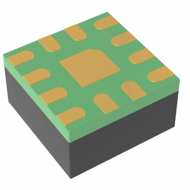
- Part No.:
- LTC4126EV-ADJ#TRPBF
- Manufacturer:
- Analog Devices Inc.
- Category:
- Battery Chargers
- Package:
- 12-VFQFN Exposed Pad
- Datasheet:
-
 LTC4126EV-ADJ#TRPBF.pdf
- Description:
- IC BATT CHG LI-ION 1CELL 12LQFN
- Quantity:
- Payment:

- Shipping:

Inventory:2,466
Please send an inquiry. Send us your inquiry, and we will respond immediately.
Product details
Overview
LTC4126EV-ADJ#TRPBF from Analog Devices is a wireless single-cell Li-Ion battery charger IC with integrated 1.2V multi-mode charge-pump DC/DC regulator, programmable 1–50mA charge current via external resistor, 4.2V charge voltage, and 3.0V battery disconnect threshold. It enables compact hearing aid power systems with simultaneous wireless charging and regulated low-noise supply.
For engineers reviewing the LTC4126EV-ADJ#TRPBF datasheet, LTC4126EV-ADJ#TRPBF pinout, LTC4126EV-ADJ#TRPBF application, or LTC4126EV-ADJ#TRPBF equivalent, key selection criteria include NTC-based temperature-qualified charging, dual-mode (50kHz/75kHz) switching to avoid audible noise, 12-lead 2mm × 2mm LQFN package with exposed GND pad, and differential undervoltage current limiting (DUVCL) for stable operation under variable coupling conditions.
Technical Context
The LTC4126EV-ADJ#TRPBF integrates three functional blocks: an AC rectifier with overvoltage limit (5.5V typical VCC high limit), a linear CC/CV Li-Ion charger with 6-hour safety timer and automatic recharge at 97.5% of VCHG, and a thermally optimized multi-mode charge-pump DC/DC regulator delivering 1.2V at up to 60mA output current.
Its DC/DC operates in three modes: regulated 3:1 step-down (VBAT > 3.6V), open-loop 3:1 (3.3V < VBAT ≤ 3.6V), and 2:1 step-down (VBAT ≤ 3.3V), with switching frequencies fixed at 50kHz or 75kHz depending on mode-ensuring no spectral energy falls within the 20Hz–20kHz audio band.
Key Specifications
| Parameter | Value and Actual Design Meaning |
|---|---|
| Charge Voltage | 4.2V ±21mV - precise termination point for standard Li-Ion cells, minimizing stress and maximizing cycle life. |
| Programmable Charge Current | 1mA to 50mA - set by single external resistor (RPROG = 100·1.1V/ICHG − 2.2kΩ), enabling fine-grained power budgeting for ultra-low-power wearables. |
| DC/DC Output Voltage | 1.2V ±40mV (typical) - tightly regulated rail for hearing aid ASICs, with load regulation maintained across 0–60mA output range. |
| Battery Disconnect Threshold | 3.0V ±70mV - prevents deep discharge damage by isolating battery from system loads below safe operating voltage. |
| NTC Temperature Monitoring | Voltage thresholds at 76.5% (cold) and 34.9% (hot) of VCC - enables safe charging between ~0°C and ~40°C without external ADC or microcontroller. |
| Switching Frequency | 50kHz or 75kHz - selected automatically per battery voltage; avoids audible noise and simplifies EMI filtering. |
| Package | 12-lead 2mm × 2mm × 0.74mm LQFN with exposed GND pad - supports high thermal conductivity and minimal PCB footprint for space-constrained implants and wearables. |
Pinout & Package
Thermally enhanced 12-lead LQFN (2mm × 2mm × 0.74mm) with exposed GND pad (Pin 13) requiring solder connection to PCB ground for electrical integrity and thermal performance.
| Pin/Terminal | Circuit Role | Design Meaning |
|---|---|---|
| NTC (Pin 1) | Thermistor input | Monitors battery temperature via voltage divider; suspends charging if outside safe range (0°C–40°C typical), referenced to VCC. |
| EN (Pin 2) | Digital enable input | Active-high logic control (VIH ≥ 1.1V) for DC/DC; overrides PBEN when asserted; tie to BAT for always-on operation. |
| PBEN (Pin 3) | Pushbutton toggle input | Internal 4MΩ pull-up enables momentary-GND button control; ignored if EN is high. |
| PROG (Pin 4) | Charge current programming | Connects to GND via precision resistor to set ICHG from 1mA to 50mA; 1% tolerance recommended. |
| ACPR (Pin 5) | Input power availability indicator | CMOS output referenced to OUT; high when VCC–VBAT ≥ 80mV (typ), low when ≤27mV (typ); requires DC/DC enabled. |
| CHRG (Pin 6) | Open-drain charge status | Indicates state via pull-down current (300µA typ): slow blink (1.14Hz) = charging, fast blink (4.58Hz) = fault, pulled low = done, Hi-Z = no input power. |
| ACIN (Pin 7) | AC receive coil interface | Connects to parallel LC tank for wireless power reception; internal rectifier feeds VCC; short to GND if unused. |
| BAT (Pin 8) | Battery connection | Direct connection to single-cell Li-Ion anode; powers DC/DC and receives charge current; decouple with 1µF ceramic if DC/DC active during charge. |
| STAT2 (Pin 9), STAT1 (Pin 10) | Charging status logic outputs | CMOS outputs referenced to OUT; encode charge/fault states jointly with ACPR; inactive if DC/DC disabled. |
| VCC (Pin 11) | Rectified input supply | Output of internal AC rectifier (from ACIN) or DC input node; clamped to 5.5V max; powers internal circuitry and charger. |
| OUT (Pin 12) | DC/DC regulated output | Delivers 1.2V to load; requires ≥2.2µF low-ESR ceramic capacitor placed adjacent to pin for stability and transient response. |
| GND (Pin 13) | Ground reference & thermal pad | Exposed copper pad on package underside; must be soldered to PCB ground plane for electrical return and thermal dissipation (θJA = 92°C/W). |
Key Features
| Feature | Design Value |
|---|---|
| Multi-mode charge-pump DC/DC | Three operating modes (3:1 regulated, 3:1 open-loop, 2:1) maintain 1.2V output across full battery range (3.0V–4.25V) while optimizing efficiency and noise. |
| Differential undervoltage current limiting (DUVCL) | Gradually reduces charge current as VCC–VBAT drops from 154mV to 116mV-prevents oscillatory charging under weak magnetic coupling in wireless systems. |
| Temperature-qualified charging | Integrated NTC comparators with 1.5% hysteresis eliminate need for external temperature sensing circuitry or firmware intervention. |
| Low-noise 50kHz/75kHz switching | Fixed-frequency operation avoids audio-band interference critical for hearing aid signal chains and sensitive analog front-ends. |
| Ultra-low quiescent current | 4µA BAT quiescent current (DC/DC off, VBAT = 4.25V) extends shelf life and runtime in intermittently powered wearables. |
Applications
| Hearing Aid Power System | Wireless Charging Earbud | |
|---|---|---|
Use Scenario: Compact in-ear device requiring simultaneous wireless charging and ultra-low-noise 1.2V supply for audio DSP and RF transceiver. IC Role / Device Role / Timing Role: Dual-role IC providing CC/CV Li-Ion charging and regulated step-down conversion, eliminating need for separate charger + LDO. Use Value: Enables sub-10mm form factor with 60mA DC/DC output, 3.0V disconnect protection, and NTC-based thermal safety-no external supervision required. |
Use Scenario: True wireless stereo (TWS) earbud case with integrated wireless transmitter and earbud receiver using resonant coupling. IC Role / Device Role / Timing Role: Receiver-side power management IC handling AC rectification, battery charging, and system rail generation from same coil. Use Value: DUVCL ensures stable charging despite variable coil alignment; 50kHz/75kHz switching avoids interference with Bluetooth audio transmission. |
|
| IoT Medical Sensor Patch | Low-Power Wearable Tracker | |
Use Scenario: Disposable skin-adhered patch monitoring vital signs for 7+ days, recharged wirelessly via bedside pad. IC Role / Device Role / Timing Role: Primary power IC managing energy harvesting from wireless field, battery health, and regulated supply for sensor hub. Use Value: 1mA minimum charge current enables trickle replenishment from low-power transmitters; 6-hour safety timer prevents overcharge in unattended use. |
Use Scenario: Fitness tracker with coin-cell-sized Li-Ion battery and daily wireless charging via cradle. | IC Role / Device Role / Timing Role: Integrated charger + DC/DC eliminates discrete regulators and reduces BOM count by two components. Use Value: 2mm × 2mm LQFN package saves >30% board area vs. traditional charger + LDO solution; pushbutton control (PBEN) enables user-initiated power-on. |
Equivalent & Alternatives
The following parts are listed as comparable options for similar wireless Li-Ion charging applications.
| Alternative Part | Technical Difference | Application Difference | Selection Advice |
|---|---|---|---|
| BQ51013BRGER | Single-chip Qi-compliant receiver with integrated 5V buck-boost DC/DC; no programmable charge current; fixed 4.2V charge voltage; larger 3mm × 3mm QFN package. | Designed for Qi-standard consumer electronics; lacks NTC input and low-noise 1.2V rail; unsuitable for hearing aids due to higher EMI and voltage mismatch. | Select only if Qi compliance and 5V system rail are mandatory; not drop-in for 1.2V ASIC supply or medical-grade thermal safety. |
| MAX77751EWA+T | High-efficiency buck-boost charger with I²C interface, 1.8V–5.5V output; requires external MCU for configuration; no integrated NTC comparator; 16-pin WLP package. | Targeted at smartphones/tablets with host-controlled power management; adds software complexity and PCB area vs. LTC4126EV-ADJ#TRPBF's autonomous operation. | Choose when dynamic output voltage adjustment or telemetry logging is needed; avoid when autonomous, ultra-compact, or low-EMI operation is primary. |
Compared with BQ51013BRGER and MAX77751EWA+T, the LTC4126EV-ADJ#TRPBF uniquely combines autonomous NTC-based thermal safety, ultra-low-noise 1.2V DC/DC output, and DUVCL for robust wireless charging in miniaturized medical devices-without requiring host MCU or Qi infrastructure.
Availability
LTC4126EV-ADJ#TRPBF is available at Aetrix Electronics and suitable for hearing aids, wireless headsets, IoT wearables, and low-power medical sensors requiring stable component supply, RoHS-compliant packaging, and guaranteed long-term availability.
Supply support for LTC4126EV-ADJ#TRPBF includes scheduled delivery planning, volume procurement assistance, BOM continuity management, traceable sourcing, and lifecycle availability coordination for OEM customers, industrial embedded developers, connected-device designers, and electronics production programs.
Manufacturer
Analog Devices, Inc. is a global leader in high-performance analog, mixed-signal, and digital signal processing semiconductors, serving industrial, automotive, communications, and healthcare markets.
The LTC4126EV-ADJ#TRPBF belongs to Analog Devices' Power by Linear™ wireless charging product line, designed specifically for ultra-low-power, size-constrained wearable and implantable medical devices requiring autonomous, thermally safe, and EMI-optimized power management.
FAQ
What is the function of the PROG pin on the LTC4126EV-ADJ#TRPBF?
The PROG pin on the LTC4126EV-ADJ#TRPBF sets the battery charge current via an external resistor connected to GND. Using the formula RPROG = (100 × 1.1V)/ICHG − 2.2kΩ, designers can precisely program ICHG from 1mA to 50mA. For example, a 12.4kΩ resistor yields ~7.5mA charge current. The LTC4126EV-ADJ#TRPBF uses this pin to configure its linear CC/CV charger without requiring digital interface or trimming.
How does the LTC4126EV-ADJ#TRPBF handle low-input-power conditions during wireless charging?
The LTC4126EV-ADJ#TRPBF employs Differential Undervoltage Current Limiting (DUVCL) to gracefully scale charge current as VCC–VBAT drops from 154mV to 116mV-avoiding abrupt shutdowns common with basic DUVLO circuits. This prevents oscillatory charging under weak magnetic coupling. When current falls below 40% of programmed value, the CHRG pin blinks fast (4.58Hz) to indicate DUVCL activation. The LTC4126EV-ADJ#TRPBF maintains system stability without external intervention.
Can the LTC4126EV-ADJ#TRPBF operate without wireless power input?
Yes-the LTC4126EV-ADJ#TRPBF supports dual power sources. When ACIN is grounded, a DC voltage (2.7V–5.5V) applied directly to the VCC pin powers both the charger and internal circuitry. The IC functions identically: charging proceeds at programmed current, DC/DC delivers 1.2V, and all protections (NTC, DUVCL, safety timer) remain fully active. This flexibility allows the same LTC4126EV-ADJ#TRPBF design to serve wired and wireless charging variants.
What is the purpose of the exposed pad (Pin 13) on the LTC4126EV-ADJ#TRPBF package?
The exposed pad (Pin 13) on the LTC4126EV-ADJ#TRPBF is a dedicated GND connection that must be soldered to the PCB ground plane. It serves two critical roles: (1) providing low-impedance electrical return for internal currents, and (2) dissipating heat-enabling θJA = 92°C/W. Omitting this connection risks thermal shutdown, voltage regulation drift, and reduced reliability. The LTC4126EV-ADJ#TRPBF datasheet explicitly requires soldering this pad for guaranteed operation across –20°C to 85°C.
How does the LTC4126EV-ADJ#TRPBF indicate charging status and faults?
The LTC4126EV-ADJ#TRPBF provides status through three complementary interfaces: (1) CHRG pin (open-drain) blinks slowly (1.14Hz) during charging, fast (4.58Hz) for faults (NTC, bad battery, DUVCL), pulls low when done, or floats with no input; (2) ACPR goes high when VCC–VBAT ≥ 80mV; (3) STAT1/STAT2 encode states jointly (e.g., 0/1 = charging) when DC/DC is enabled. All indicators are implemented autonomously within the LTC4126EV-ADJ#TRPBF-no firmware required.
LTC4126EV-ADJ#TRPBF Specifications
- Product attributes
- Attribute value
- Manufacturer:
- Analog Devices Inc.
- Series:
- -
- Package/Case:
- 12-VFQFN Exposed Pad
- Packaging:
- Tape & Reel (TR)
- Product Status:
- Active
- Battery Chemistry:
- Lithium Ion
- Number of Cells:
- 1
- Current - Charging:
- Constant
- Programmable Features:
- Current, Timer
- Fault Protection:
- Undervoltage
- Charge Current - Max:
- 50mA
- Battery Pack Voltage:
- 4.2V
- Voltage - Supply (Max):
- 5.5V
- Interface:
- -
- Operating Temperature:
- -20°C ~ 85°C (TJ)
- Grade:
- -
- Qualification:
- -
- Mounting Type:
- Surface Mount
- Supplier Device Package:
- 12-LQFN (2x2)
LTC4126EV-ADJ#TRPBF FAQ
1.How can I place an order for LTC4126EV-ADJ#TRPBF through Aetrix?
Please submit a Request for Quotation (RFQ) for LTC4126EV-ADJ#TRPBF on Aetrix. Our sales agent will provide a competitive quotation and guide you through the order confirmation once you accept the terms.
2.Are the price and stock information for LTC4126EV-ADJ#TRPBF reliable?
The price and inventory of LTC4126EV-ADJ#TRPBF are updated periodically and may fluctuate due to market conditions. Stock and pricing data are typically refreshed every 24 hours. Quotation validity for LTC4126EV-ADJ#TRPBF is usually 5 days.
3.What payment methods are accepted for LTC4126EV-ADJ#TRPBF?
We accept Wire Transfer, PayPal, Credit Card, Western Union, MoneyGram, and Escrow for LTC4126EV-ADJ#TRPBF transactions.
Note: Certain payment methods may incur a processing fee.
4.How is shipping managed for LTC4126EV-ADJ#TRPBF?
LTC4126EV-ADJ#TRPBF orders can be shipped via leading logistics carriers, including DHL, UPS, FedEx, TNT, or Registered Mail.
Once your LTC4126EV-ADJ#TRPBF order is processed, you will receive an email with the shipment details and tracking number.
Note: Tracking information may take up to 24 hours to appear. Express delivery typically takes 3–5 business days.
5.How can I obtain technical support or documentation for LTC4126EV-ADJ#TRPBF?
For technical support, including LTC4126EV-ADJ#TRPBF datasheets, pinout diagrams, or application guidance, please contact our engineering support team. They can provide detailed documentation and assistance for your LTC4126EV-ADJ#TRPBF requirements.
6.How does Aetrix verify that LTC4126EV-ADJ#TRPBF is sourced from the original manufacturer or authorized distributors?
All LTC4126EV-ADJ#TRPBF products on Aetrix are procured from qualified distributors and authorized channels. Our dedicated quality assurance team conducts strict verification, including traceability checks and, if necessary, third-party testing. This ensures that LTC4126EV-ADJ#TRPBF meets industry standards.
7.What is the process for return or replacement of LTC4126EV-ADJ#TRPBF?
All LTC4126EV-ADJ#TRPBF units undergo pre-shipment inspection (PSI). If there is an issue with LTC4126EV-ADJ#TRPBF, returns or replacements are accepted under the following conditions:
1.Quantity discrepancies, incorrect items, or visible external defects (such as breakage or corrosion), acknowledged by Aetrix.
2.The issue is reported within 90 days of delivery.
3.The LTC4126EV-ADJ#TRPBF part is unused and in its original packaging.
Return procedure for LTC4126EV-ADJ#TRPBF:
1.Submit a request within 90 days.
2.Obtain a Return Material Authorization (RMA) from Aetrix.
LTC4126EV-ADJ#TRPBF Tags

-
BQ21040DBVR
Texas Instruments

-
MCP73812T-420I/OT
Microchip Technology
-
MCP73831T-2ACI/OT
Microchip Technology
-
MCP73832T-2ACI/OT
Microchip Technology
-
MCP73831T-2DCI/OT
Microchip Technology
-
MCP73832T-2DCI/OT
Microchip Technology
-
MCP73831T-2ATI/OT
Microchip Technology
-
MCP73832T-2ATI/OT
Microchip Technology
-
MCP73831T-5ACI/OT
Microchip Technology

-
MCP73832T-2ACI/MC
Microchip Technology
-
MCP73831T-2ACI/MC
Microchip Technology
-
MCP73831T-2ATI/MC
Microchip Technology
Tech Hub

A practical engineering guide to 3.3V and 5V logic compatibility, input thresholds, resistor dividers, translator ICs, MOSFET level shifting, I2C pull-ups, timing limits and power-sequencing risks.

The 74HC595 uses push-pull logic outputs, while the TPIC6B595 uses 50 V open-drain DMOS sinks for higher-power loads. This guide compares timing, current limits, 3.3 V interfacing, load wiring, thermal…

The 74HC595 converts serial data into eight stable parallel outputs. This guide covers pin functions, shift and storage timing, OE and MR behavior, drive-current limits, cascading, voltage compatibilit…

A technical comparison of level-sensitive latches and edge-triggered flip-flops, covering timing windows, setup and hold limits, master–slave operation, time borrowing, race-through, HDL inference and…

A D latch stores one bit while Enable controls when data can pass. This reference covers gate-level operation, truth tables, transparency, setup and hold timing, LE versus OE, common ICs and practical …

An SR latch stores one bit through cross-coupled feedback. This engineering reference covers NOR and NAND implementations, truth tables, forbidden-state recovery, gated operation, switch debouncing, fa…

Latch circuits retain one bit through feedback. This technical reference covers SR and D latches, truth tables, transparency, timing limits, latch-versus-flip-flop behavior, applications and common log…

An engineering guide to LED driver operation, constant-current and constant-voltage outputs, linear and switching topologies, dimming, IC selection, calculations, replacement compatibility, and fault c…

Operational amplifier guide covering op amp basics, feedback, ideal vs real op amps, common configurations, buffer circuits, offset, bias current, gain-bandwidth, slew rate, rail-to-rail limits and sel…

Jumper cables guide covering safe connection order, red and black clamp placement, final ground connection, cable gauge, length, clamp quality, copper vs CCA cables, jump starter comparison and battery…


