
 My Inquiry
 My Account


Analog Devices Inc. LTC4310CDD-2#PBF
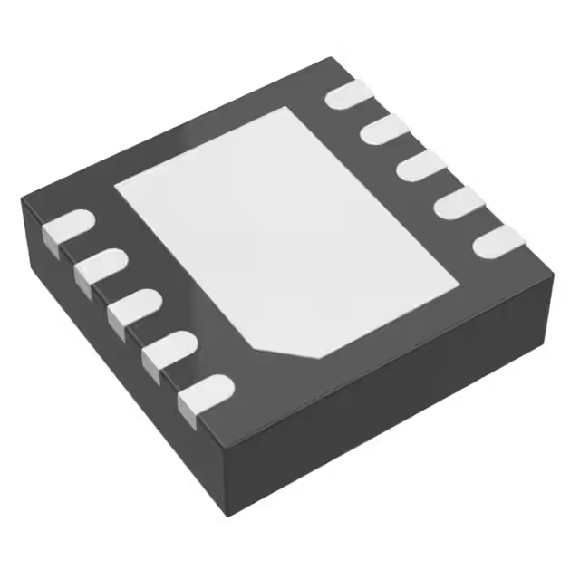
- Part No.:
- LTC4310CDD-2#PBF
- Manufacturer:
- Analog Devices Inc.
- Category:
- Digital Isolators
- Package:
- 10-WFDFN Exposed Pad
- Datasheet:
-
 LTC4310CDD-2#PBF.pdf
- Description:
- DIGITAL ISOLATOR 2CH I2C 10DFN
- Quantity:
- Payment:

- Shipping:

Inventory:1,119
Please send an inquiry. Send us your inquiry, and we will respond immediately.
Product details
Overview
LTC4310CDD-2#PBF from Analog Devices (formerly Linear Technology) is a bidirectional I²C isolator IC designed to enable robust, hot-swappable communication across galvanically isolated I²C buses. It supports 400kHz operation, provides ±5kV HBM ESD protection, integrates rise time accelerators for heavily loaded buses, and features stuck bus recovery with automatic clock generation and STOP bit insertion. It is used in isolated power supply monitoring and PoE-powered device management.
For engineers reviewing the LTC4310CDD-2#PBF datasheet, LTC4310CDD-2#PBF pinout, LTC4310CDD-2#PBF application, or LTC4310CDD-2#PBF equivalent, key selection criteria include maximum SCL frequency (400kHz), isolation barrier interface (transformer or capacitor-coupled), thermal shutdown threshold (150°C), EN-controlled shutdown current (≤0.1µA), and READY open-drain status signaling.
Technical Context
The LTC4310CDD-2#PBF implements event-driven differential pulse transmission over TXP/TXN and RXP/RXN pins, using 1.25V pseudo-differential pulses with ≤35ns width and ≤3ns rise/fall times. Its logic detection circuitry distinguishes local bus activity from self-driven outputs, enabling seamless arbitration, clock stretching, and ACK/NACK propagation across isolation barriers.
It enforces controlled SDA/SCL rising edge rates of 2–6.9 V/µs (depending on VCC) and activates IBOOST (2–6mA) above 0.45•VCC to meet I²C rise time specs under high bus capacitance (up to 800pF). Stuck bus recovery initiates after 37ms low state, issuing up to sixteen SCL clocks and a STOP bit before releasing drivers.
Key Specifications
| Parameter | Value and Actual Design Meaning |
|---|---|
| Max SCL Frequency | 400kHz - enables fast I²C systems compliant with Fast-mode Plus timing budgets. |
| Supply Voltage Range | 3V to 5.5V - supports direct interfacing with 3.3V and 5V I²C domains without level shifters. |
| Shutdown Current | ≤0.1µA at EN = 0V - minimizes standby power in battery-backed or energy-sensitive systems. |
| Rise Time Acceleration | IBOOST = 2–6mA - actively pulls SDA/SCL during rising edges to overcome >400pF bus loads. |
| ESD Protection | ±5kV HBM - protects against handling-induced transients in industrial and telecom environments. |
| Thermal Shutdown | Triggers at 150°C, releases at 130°C - prevents permanent damage during sustained overload or poor heatsinking. |
| Stuck Bus Timeout | 37ms - detects and recovers from bus lockups caused by faulty slaves or wiring faults. |
Pinout & Package
Package: 10-lead (3mm × 3mm) plastic DFN with exposed pad (Pin 11), rated for 0°C to 70°C ambient operation.
| Pin/Terminal | Circuit Role | Design Meaning |
|---|---|---|
| EN (1) | Enable input | Active-high control: drives device into ultra-low-current shutdown (<0.1µA) when pulled low. |
| SDA (2) | Bidirectional I²C data line | Open-drain output with 0.35V regulated low-level drive and rise time acceleration above 0.45•VCC. |
| SCL (3) | Bidirectional I²C clock line | Functionally identical to SDA; supports clock stretching and arbitration transparency across isolation. |
| READY (4) | Open-drain status output | Pulls low only when device is actively synchronizing local and remote bus states; indicates link readiness. |
| GND (5) | Signal ground reference | Common return for internal circuitry; exposed pad may be connected to GND for thermal enhancement. |
| TXN (6) | Negative transmit output | Drives negative side of transformer primary or coupling capacitor; forms differential pair with TXP. |
| TXP (7) | Positive transmit output | Drives positive side of transformer primary or coupling capacitor; 1.25V pseudo-differential pulse source. |
| VCC (8) | Power supply input | Requires ≥0.01µF bypass capacitor to GND; UVLO triggers below 2.1V with 90–270mV hysteresis. |
| RXP (9) | Positive receive input | Differential receiver input; rejects common-mode transients <500mV; requires ≥47pF coupling capacitor. |
| RXN (10) | Negative receive input | Complements RXP; differential input impedance 13–20kΩ; enables noise-immune signal recovery. |
Key Features
| Feature | Design Value |
|---|---|
| Transformer or capacitor isolation | Enables >1500V isolation using low-cost Ethernet transformers or ceramic capacitors-no optocouplers required. |
| Hot-swap ready I²C interface | Prevents data corruption during live card insertion/removal via synchronized START/STOP detection and bus idle monitoring. |
| Controlled rise rate limiting | Regulates SDA/SCL rise to (0.35•VCC)/300ns for LTC4310-2-ensures deterministic skew between isolated buses. |
| Autonomous stuck bus recovery | Generates up to 16 clocks + STOP bit without host intervention-restores bus functionality after slave lockup. |
| Ready-status signaling | READY pin asserts low only after both local and remote buses achieve simultaneous STOP/idle-guarantees synchronization. |
Applications
| Isolated Power Supply Monitoring | Hot-Swappable Server Blades |
|---|---|
Use Scenario: Monitoring voltage, temperature, and fault status of isolated DC-DC converters in telecom rectifiers. IC Role / Device Role / Timing Role: I²C isolator bridging primary-side controller and secondary-side PMBus slave devices across reinforced isolation barrier. Use Value: Maintains full SMBus protocol transparency-including clock stretching and multi-master arbitration-while meeting IEC 62368-1 creepage/clearance requirements. |
Use Scenario: Enabling safe insertion/removal of compute blades into live backplane I²C management bus in data center chassis. IC Role / Device Role / Timing Role: Bidirectional I²C repeater with bus idle detection and READY handshake to prevent transaction corruption during hot-plug events. Use Value: Eliminates need for software reset or bus reinitialization after blade insertion-reduces system downtime and firmware complexity. |
| Power-over-Ethernet (PoE) PD Management | Industrial Sensor Node Isolation |
Use Scenario: Communicating with PoE-powered endpoint devices (e.g., IP cameras, wireless APs) while maintaining isolation from PSE-side control logic. IC Role / Device Role / Timing Role: I²C isolator linking IEEE 802.3af/at-compliant PSE controller to isolated PD-side configuration registers and fault reporting. Use Value: Supports 400kHz Fast-mode Plus timing for rapid classification and power negotiation-critical for multi-port PSE scalability. |
Use Scenario: Interfacing isolated analog sensor front-ends (e.g., RTD, strain gauge) to microcontroller-based data loggers in high-noise factory environments. IC Role / Device Role / Timing Role: Galvanic barrier for I²C sensor readout, rejecting >20kV/µs common-mode transients induced by motor drives or welding equipment. Use Value: Prevents ground loop currents from corrupting 16-bit ADC readings-enables stable 0.1% measurement accuracy in EMC-critical applications. |
Equivalent & Alternatives
The following parts are listed as comparable options for similar I²C isolation applications.
| Alternative Part | Technical Difference | Application Difference | Selection Advice |
|---|---|---|---|
| ISO1540DR | 2-channel, 1Mbps digital isolator with integrated I²C logic; no rise time acceleration; max 100kHz SCL due to propagation delay. | Limited to standard-mode I²C; lacks autonomous stuck bus recovery and READY status signaling. | Select ISO1540DR only for cost-sensitive, low-frequency (<100kHz), non-hot-swap applications where external pull-up optimization is acceptable. |
| ADUM1250ARZ | Two-channel iCoupler® digital isolator; supports 1MHz data rate but requires external I²C bus buffers and level shifters. | No native I²C protocol awareness-clock stretching and arbitration must be handled externally; no built-in thermal shutdown. | Choose ADUM1250ARZ when system already uses ADI isolators and custom logic can manage I²C timing constraints and fault recovery. |
Compared with ISO1540DR and ADUM1250ARZ, the LTC4310CDD-2#PBF delivers full I²C protocol transparency at 400kHz, eliminates external buffer components, and embeds critical system-level functions-stuck bus recovery, READY handshake, and rise time acceleration-reducing BOM count and firmware overhead.
Availability
LTC4310CDD-2#PBF is available at Aetrix Electronics and suitable for isolated power management, hot-swappable server infrastructure, and Power-over-Ethernet endpoint design requiring stable component supply and long-term industrial lifecycle support.
Supply support for LTC4310CDD-2#PBF includes scheduled delivery planning, volume procurement assistance, BOM continuity management, traceable sourcing, and lifecycle availability coordination for OEM customers, industrial embedded developers, connected-device designers, and electronics production programs.
Manufacturer
Analog Devices, Inc. (acquired Linear Technology in 2017) is a global leader in high-performance analog, mixed-signal, and digital signal processing semiconductors.
The LTC4310CDD-2#PBF belongs to Linear's Hot Swap™ and I²C isolation product line, engineered specifically for robust, protocol-transparent galvanic isolation in mission-critical power and communications infrastructure.
FAQ
What is the maximum I²C clock frequency supported by the LTC4310CDD-2#PBF?
The LTC4310CDD-2#PBF supports a maximum SCL clock frequency of 400kHz, as specified in its Electrical Characteristics table. This distinguishes it from the LTC4310-1 variant (100kHz) and enables compatibility with Fast-mode Plus I²C systems. The device maintains full protocol compliance-including clock stretching and arbitration-at this speed, provided bus rise times are maintained via proper pull-up resistor selection and rise time accelerator activation.
Does the LTC4310CDD-2#PBF require external pull-up resistors on SDA and SCL lines?
Yes, the LTC4310CDD-2#PBF requires external pull-up resistors on both SDA and SCL lines-typically connected to the local bus supply (≥VCC). The maximum allowable resistance depends on bus capacitance and target frequency: for 400kHz operation, Figure 3 in the datasheet specifies RBUS(MAX) ≈ 4.3kΩ at 3.3V with 40pF load. The device's rise time accelerators activate above 0.45•VCC to assist these resistors, but they do not eliminate the need for them.
How does the LTC4310CDD-2#PBF handle a stuck I²C bus condition?
The LTC4310CDD-2#PBF monitors SDA and SCL for low-state duration; if both remain low for 37ms, it disables its drivers, transmits a stuck-bus alert across the isolation barrier, then issues up to sixteen SCL clock pulses followed by a STOP bit. This autonomous recovery sequence occurs without host intervention and resets all connected slaves. The READY pin releases high during stuck-bus mode and reasserts low only after both buses achieve simultaneous STOP/idle.
Can the LTC4310CDD-2#PBF be used with capacitive isolation instead of transformers?
Yes, the LTC4310CDD-2#PBF supports capacitive isolation using ceramic coupling capacitors on TXP/TXN and RXP/RXN. The datasheet recommends CRXP/CRXN ≥ 47pF and ≥10× board trace parasitic capacitance (CPAR). Capacitive coupling is suitable for lower-voltage isolation (e.g., <500V) and simplifies layout versus transformer-based solutions, though transformer coupling remains preferred for >1500V applications like PoE or industrial AC/DC supplies.
What is the function of the READY pin on the LTC4310CDD-2#PBF?
The READY pin on the LTC4310CDD-2#PBF is an open-drain output that pulls low only when the device has successfully synchronized the local and remote I²C buses-i.e., after detecting simultaneous STOP bits or bus idle states on both sides. It signals to the host system that bidirectional communication is active and stable. During startup, thermal shutdown, EN-driven shutdown, or stuck-bus recovery, READY floats high, providing unambiguous link status without polling.
LTC4310CDD-2#PBF Specifications
- Product attributes
- Attribute value
- Manufacturer:
- Analog Devices Inc.
- Series:
- -
- Package/Case:
- 10-WFDFN Exposed Pad
- Packaging:
- Tube
- Product Status:
- Active
- Technology:
- Magnetic Coupling
- Type:
- I2C
- Isolated Power:
- No
- Number of Channels:
- 2
- Inputs - Side 1/Side 2:
- 1/1
- Channel Type:
- Unidirectional
- Voltage - Isolation:
- -
- Common Mode Transient Immunity (Min):
- 20kV/µs
- Data Rate:
- 400kHz
- Propagation Delay tpLH / tpHL (Max):
- -
- Pulse Width Distortion (Max):
- -
- Rise / Fall Time (Typ):
- 1ns, 1ns
- Voltage - Supply:
- 3V ~ 5.5V
- Grade:
- -
- Qualification:
- -
- Operating Temperature:
- 0°C ~ 70°C
- Mounting Type:
- Surface Mount
- Supplier Device Package:
- 10-DFN (3x3)
LTC4310CDD-2#PBF FAQ
1.How can I place an order for LTC4310CDD-2#PBF through Aetrix?
Please submit a Request for Quotation (RFQ) for LTC4310CDD-2#PBF on Aetrix. Our sales agent will provide a competitive quotation and guide you through the order confirmation once you accept the terms.
2.Are the price and stock information for LTC4310CDD-2#PBF reliable?
The price and inventory of LTC4310CDD-2#PBF are updated periodically and may fluctuate due to market conditions. Stock and pricing data are typically refreshed every 24 hours. Quotation validity for LTC4310CDD-2#PBF is usually 5 days.
3.What payment methods are accepted for LTC4310CDD-2#PBF?
We accept Wire Transfer, PayPal, Credit Card, Western Union, MoneyGram, and Escrow for LTC4310CDD-2#PBF transactions.
Note: Certain payment methods may incur a processing fee.
4.How is shipping managed for LTC4310CDD-2#PBF?
LTC4310CDD-2#PBF orders can be shipped via leading logistics carriers, including DHL, UPS, FedEx, TNT, or Registered Mail.
Once your LTC4310CDD-2#PBF order is processed, you will receive an email with the shipment details and tracking number.
Note: Tracking information may take up to 24 hours to appear. Express delivery typically takes 3–5 business days.
5.How can I obtain technical support or documentation for LTC4310CDD-2#PBF?
For technical support, including LTC4310CDD-2#PBF datasheets, pinout diagrams, or application guidance, please contact our engineering support team. They can provide detailed documentation and assistance for your LTC4310CDD-2#PBF requirements.
6.How does Aetrix verify that LTC4310CDD-2#PBF is sourced from the original manufacturer or authorized distributors?
All LTC4310CDD-2#PBF products on Aetrix are procured from qualified distributors and authorized channels. Our dedicated quality assurance team conducts strict verification, including traceability checks and, if necessary, third-party testing. This ensures that LTC4310CDD-2#PBF meets industry standards.
7.What is the process for return or replacement of LTC4310CDD-2#PBF?
All LTC4310CDD-2#PBF units undergo pre-shipment inspection (PSI). If there is an issue with LTC4310CDD-2#PBF, returns or replacements are accepted under the following conditions:
1.Quantity discrepancies, incorrect items, or visible external defects (such as breakage or corrosion), acknowledged by Aetrix.
2.The issue is reported within 90 days of delivery.
3.The LTC4310CDD-2#PBF part is unused and in its original packaging.
Return procedure for LTC4310CDD-2#PBF:
1.Submit a request within 90 days.
2.Obtain a Return Material Authorization (RMA) from Aetrix.
LTC4310CDD-2#PBF Tags

-
ISO1212DBQR
Texas Instruments
-
ISO6721BDR
Texas Instruments
-
SI8710AC-B-ISR
Skyworks Solutions Inc.
-
ISO7720FDR
Texas Instruments
-
ISO7721DR
Texas Instruments
-
ISO7721FDR
Texas Instruments
-
SI8710CC-B-ISR
Skyworks Solutions Inc.
-
ISO6741FQDWRQ1
Texas Instruments

-
ISO7721DWVR
Texas Instruments
-
ISO7762FDBQR
Texas Instruments

-
ISO7741DWR
Texas Instruments
-
ISO7741FDWR
Texas Instruments
Tech Hub

A practical engineering guide to 3.3V and 5V logic compatibility, input thresholds, resistor dividers, translator ICs, MOSFET level shifting, I2C pull-ups, timing limits and power-sequencing risks.

The 74HC595 uses push-pull logic outputs, while the TPIC6B595 uses 50 V open-drain DMOS sinks for higher-power loads. This guide compares timing, current limits, 3.3 V interfacing, load wiring, thermal…

The 74HC595 converts serial data into eight stable parallel outputs. This guide covers pin functions, shift and storage timing, OE and MR behavior, drive-current limits, cascading, voltage compatibilit…

A technical comparison of level-sensitive latches and edge-triggered flip-flops, covering timing windows, setup and hold limits, master–slave operation, time borrowing, race-through, HDL inference and…

A D latch stores one bit while Enable controls when data can pass. This reference covers gate-level operation, truth tables, transparency, setup and hold timing, LE versus OE, common ICs and practical …

An SR latch stores one bit through cross-coupled feedback. This engineering reference covers NOR and NAND implementations, truth tables, forbidden-state recovery, gated operation, switch debouncing, fa…

Latch circuits retain one bit through feedback. This technical reference covers SR and D latches, truth tables, transparency, timing limits, latch-versus-flip-flop behavior, applications and common log…

An engineering guide to LED driver operation, constant-current and constant-voltage outputs, linear and switching topologies, dimming, IC selection, calculations, replacement compatibility, and fault c…

Operational amplifier guide covering op amp basics, feedback, ideal vs real op amps, common configurations, buffer circuits, offset, bias current, gain-bandwidth, slew rate, rail-to-rail limits and sel…

Jumper cables guide covering safe connection order, red and black clamp placement, final ground connection, cable gauge, length, clamp quality, copper vs CCA cables, jump starter comparison and battery…


