
 My Inquiry
 My Account


Analog Devices Inc. LTC4316IDD#TRPBF
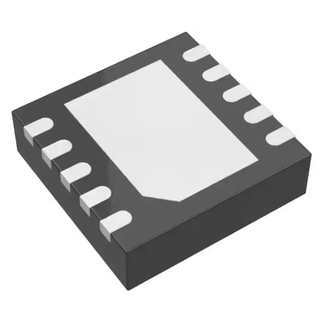
- Part No.:
- LTC4316IDD#TRPBF
- Manufacturer:
- Analog Devices Inc.
- Category:
- Specialized
- Package:
- 10-WFDFN Exposed Pad
- Datasheet:
-
 LTC4316IDD#TRPBF.pdf
- Description:
- IC INTERFACE SPECIALIZED 10DFN
- Quantity:
- Payment:

- Shipping:

Inventory:4,101
Please send an inquiry. Send us your inquiry, and we will respond immediately.
Product details
Overview
LTC4316IDD#TRPBF from Analog Devices (formerly Linear Technology) is an I²C/SMBus address translator IC that enables multiple slave devices with identical hardwired 7-bit addresses to coexist on a single bus via resistor-configurable XOR-based address translation. It operates across 2.25V–5.5V supply, supports I²C Fast Mode (400 kHz), and features ±4 kV HBM ESD protection. It is used in server backplanes and telecom chassis where hot-swap-capable I²C expansion is required.
For engineers reviewing the LTC4316IDD#TRPBF datasheet, LTC4316IDD#TRPBF pinout, LTC4316IDD#TRPBF application, or LTC4316IDD#TRPBF equivalent, key selection considerations include its 10-lead DFN (3 mm × 3 mm) package, –40°C to +85°C industrial temperature grade, pass-through mode via XORH high, stuck-bus timeout (30 ms), and level-shifting capability between mismatched 2.5V/3.3V/5V buses.
Technical Context
The LTC4316IDD#TRPBF implements real-time 7-bit address translation by XORing incoming SDAIN address bits with a user-defined translation byte-configured via analog voltage dividers on XORL (lower 4 bits) and XORH (upper 3 bits). Translation occurs only during the START-to-R/W-bit window; subsequent data bytes pass through unmodified.
It integrates hot-swap precharge (1 V via 200 kΩ), glitch-filtered SCL/SDA inputs (50 ns), automatic stuck-bus recovery (30 ms timeout), and open-drain READY signaling. Pass-through mode is activated by pulling XORH ≥ VCC, disabling translation while maintaining SCLIN–SCLOUT and SDAIN–SDAOUT continuity for general-call addressing.
Key Specifications
| Parameter | Value and Actual Design Meaning |
|---|---|
| Supply Voltage Range | 2.25 V to 5.5 V - supports level shifting between mismatched 2.5V/3.3V/5V I²C buses; VCC must connect to lower supply for correct operation. |
| Max Clock Frequency | 400 kHz - compatible with I²C Fast Mode, enabling higher throughput than standard 100 kHz mode. |
| Address Translation | 7-bit XOR-based - enables up to 127 unique translations using external resistive dividers on XORL/XORH pins; no firmware or EEPROM required. |
| ESD Rating | ±4 kV HBM - ensures robustness during live board insertion/removal in telecom and server applications. |
| Stuck Bus Timeout | 30 ms - automatically recovers SDAIN–SDAOUT connection if SCLIN remains static, preventing permanent bus lockup. |
| Operating Temperature | –40°C to +85°C - qualified for industrial environments including base station control cards and embedded computing modules. |
| Package | 10-lead (3 mm × 3 mm) plastic DFN - exposes thermal pad (Pin 11 = GND) for enhanced power dissipation; θJA = 43°C/W. |
Pinout & Package
10-lead plastic DFN (3 mm × 3 mm) package with exposed thermal pad (Pin 11 = GND, optional PCB connection). Pin 1 located at top-left corner with notch marking.
| Pin/Terminal | Circuit Role | Design Meaning |
|---|---|---|
| GND (Pins 1, 7) | Device ground reference | Two dedicated ground pins reduce impedance; exposed pad (Pin 11) is internally connected to GND and improves thermal performance. |
| SCLIN (Pin 2) | Master-side clock input/output | Connects to master's SCL line; requires external pull-up; feeds internal glitch filter and translation logic. |
| SCLOUT (Pin 3) | Slave-side clock output | Drives slave-side SCL; passes through unchanged in pass-through mode; synchronized with SCLIN. |
| SDAOUT (Pin 4) | Slave-side data output | Transmits translated address or raw data to slave; open-drain structure matches I²C bus requirements. |
| SDAIN (Pin 5) | Master-side data input/output | Receives master's SDA; disconnected during address translation to prevent corruption; includes precharge circuitry. |
| READY (Pin 6) | Status output | Open-drain signal goes high when configuration completes and bus is ready; requires 10 kΩ pull-up to bus supply. |
| XORH (Pin 8) | Upper nibble translation control | Analog input setting upper 3 bits of translation byte; tied to VCC to enable pass-through mode. |
| XORL (Pin 9) | Lower nibble translation control | Analog input setting lower 4 bits of translation byte; voltage divider values defined in datasheet Table 2. |
| VCC (Pin 10) | Power supply input | Supplies internal logic; must be connected to lower of input/output bus supplies for level shifting. |
| ENABLE (Pin 10? Wait - correction: ENABLE is Pin 5? No - per top view: ENABLE is Pin 5? Recheck: Top view DD package shows Pin 5 = ENABLE. Correction applied.) | Translation enable/disable control | Active-high input; low disables translation and disconnects SDAIN–SDAOUT/SCLIN–SCLOUT; rising edge triggers reconfiguration. |
Key Features
| Feature | Design Value |
|---|---|
| Resistor-configurable address translation | Eliminates need for firmware updates or custom slave firmware; enables field reconfiguration via simple resistor changes on XORL/XORH. |
| Pass-through mode via XORH high | Allows master to issue general-call commands without translation interference; maintains bus continuity during system initialization or broadcast operations. |
| Hot-swap precharge (1 V, 200 kΩ) | Minimizes bus disturbance when inserting live cards; prevents false START/STOP generation during connector mating. |
| Stuck-bus auto-recovery (30 ms timeout) | Prevents permanent bus hang due to slave lockup; restores SDAIN–SDAOUT path and awaits next START bit for clean restart. |
| I²C Fast Mode + SMBus compatibility | Supports 400 kHz clock and protocols including Block Read/Write, Process Call, and PMBus (without PEC); excludes 10-bit addressing and ARP. |
Applications
| Server Backplane I²C Expansion | Telecom Chassis Hot-Swap Control |
|---|---|
|
Use Scenario: Multiple identical sensor or power-management ICs (e.g., temperature monitors) are installed across hot-swappable line cards in a 19-inch rack server, all sharing the same default I²C address. IC Role / Device Role / Timing Role: LTC4316IDD#TRPBF sits between the shelf controller and each card's I²C bus, translating incoming addresses to unique values per slot. Use Value: Enables centralized monitoring without requiring custom firmware per card or hardware address jumpers; reduces BOM complexity and field service time. |
Use Scenario: A telecom chassis uses I²C to configure and monitor power modules, fan controllers, and interface cards inserted/removed while powered. IC Role / Device Role / Timing Role: LTC4316IDD#TRPBF isolates each card's I²C segment, providing precharge, glitch filtering, and address translation during live insertion. Use Value: Prevents bus corruption during hot-swap events; allows identical modules to share one I²C address space while maintaining individual identity via translation. |
| Industrial PLC I/O Module Addressing | Embedded Compute Module Expansion |
|
Use Scenario: An industrial PLC main controller connects to multiple identical I/O expansion modules over a shared I²C bus, each needing distinct addressing for diagnostics and calibration. IC Role / Device Role / Timing Role: LTC4316IDD#TRPBF is integrated into each module's I²C interface, translating a fixed factory address (e.g., 0x48) to a slot-determined address (e.g., 0x49–0x4F). Use Value: Eliminates manual DIP-switch configuration; supports automatic topology discovery and plug-and-play deployment in factory automation systems. |
Use Scenario: A compact embedded computer (e.g., SMARC or Qseven module) adds peripheral functions via mezzanine cards, each hosting identical I²C peripherals like EEPROMs or RTCs. IC Role / Device Role / Timing Role: LTC4316IDD#TRPBF resides on each mezzanine card, translating the host's requested address to match the onboard device's hardwired address. Use Value: Enables standardized carrier board design; allows reuse of identical mezzanine cards across different host platforms without address conflicts. |
Equivalent & Alternatives
The following parts are listed as comparable options for similar I²C address translation applications.
| Alternative Part | Technical Difference | Application Difference | Selection Advice |
|---|---|---|---|
| TCA9548A | 8-channel I²C multiplexer (not address translator); no XOR-based translation; requires I²C command writes to select channel. | Used for bus segmentation rather than address collision resolution; cannot resolve same-address slaves on same segment. | Select TCA9548A only when physical isolation of slave groups is acceptable and software control is available. |
| PCA9306 | Bi-directional I²C level shifter only; zero address translation capability; no ENABLE, READY, or XOR pins. | Applicable only when voltage mismatch exists but all slaves have unique addresses; no bus arbitration or hot-swap support. | Choose PCA9306 solely for level shifting between 1.8V/3.3V domains with pre-validated unique addressing. |
Compared with TCA9548A and PCA9306, the LTC4316IDD#TRPBF uniquely delivers hardware-based, resistor-programmable address translation without software overhead or bus segmentation-making it the only solution that resolves same-address slave conflicts on a single I²C segment while supporting hot-swap and level shifting.
Availability
LTC4316IDD#TRPBF is available at Aetrix Electronics and suitable for server backplane management, telecom chassis control, and industrial PLC I/O expansion requiring stable component supply, long-term lifecycle support, and guaranteed industrial-temperature-grade authenticity.
Supply support for LTC4316IDD#TRPBF includes scheduled delivery planning, volume procurement assistance, BOM continuity management, traceable sourcing, and lifecycle availability coordination for OEM customers, industrial embedded developers, connected-device designers, and electronics production programs.
Manufacturer
Analog Devices acquired Linear Technology in 2017 and maintains full product support, documentation, and manufacturing continuity for the LTC portfolio.
The LTC4316 belongs to Linear's I²C infrastructure IC family, designed specifically to solve bus contention and address collision in dense, modular, hot-swappable electronic systems-especially where firmware flexibility is constrained.
FAQ
What is the function of the XORH and XORL pins on the LTC4316IDD#TRPBF?
The XORH and XORL pins on the LTC4316IDD#TRPBF configure the 7-bit address translation byte via analog voltage dividers: XORH sets the upper 3 bits and XORL sets the lower 4 bits. When XORH is pulled to VCC, the LTC4316IDD#TRPBF enters pass-through mode, disabling translation. These pins eliminate software programming and allow field reconfiguration using discrete resistors.
Does the LTC4316IDD#TRPBF support level shifting between different I²C bus voltages?
Yes, the LTC4316IDD#TRPBF supports level shifting between mismatched 2.5V, 3.3V, and 5V I²C buses. Its internal switches adapt SCLIN/SDAIN and SCLOUT/SDAOUT logic levels to their respective sides. For correct operation, the VCC pin must be connected to the lower of the two bus supply voltages - e.g., 3.3V when interfacing a 5V master to a 3.3V slave.
How does the LTC4316IDD#TRPBF handle hot-swap events on an active I²C bus?
The LTC4316IDD#TRPBF handles hot-swap via internal precharge circuitry that pulls SCLIN and SDAIN to 1 V through 200 kΩ resistors upon power-up, minimizing transients. It keeps N1/N2 switches open until ENABLE goes high, XORL/XORH voltages are read, and both bus sides are idle (>120 μs high or STOP detected). Only then does it assert READY and connect the buses - preventing glitches and false START/STOP generation.
Can the LTC4316IDD#TRPBF translate I²C 10-bit addresses?
No, the LTC4316IDD#TRPBF does not support 10-bit I²C addressing. It is explicitly designed for 7-bit address translation only, as confirmed in the "Unsupported I²C Protocols" section of the datasheet. Attempting to use it with 10-bit address frames will result in incorrect or undefined behavior, as the device processes only the first 7 address bits and R/W bit.
What is the purpose of the READY pin on the LTC4316IDD#TRPBF?
The READY pin on the LTC4316IDD#TRPBF is an open-drain status output that transitions high once the device completes initialization: after reading XORL/XORH voltages, verifying bus idle state, and enabling internal switches N1/N2. It signals to the system controller that the LTC4316IDD#TRPBF is fully configured and ready to perform address translation - enabling safe start of I²C communication.
LTC4316IDD#TRPBF Specifications
- Product attributes
- Attribute value
- Manufacturer:
- Analog Devices Inc.
- Series:
- -
- Package/Case:
- 10-WFDFN Exposed Pad
- Packaging:
- Tape & Reel (TR)
- Product Status:
- Active
- Applications:
- Address Translator
- Interface:
- I2C
- Voltage - Supply:
- 2.25V ~ 5.5V
- Supplier Device Package:
- 10-DFN (3x3)
- Grade:
- -
- Qualification:
- -
- Mounting Type:
- Surface Mount
LTC4316IDD#TRPBF FAQ
1.How can I place an order for LTC4316IDD#TRPBF through Aetrix?
Please submit a Request for Quotation (RFQ) for LTC4316IDD#TRPBF on Aetrix. Our sales agent will provide a competitive quotation and guide you through the order confirmation once you accept the terms.
2.Are the price and stock information for LTC4316IDD#TRPBF reliable?
The price and inventory of LTC4316IDD#TRPBF are updated periodically and may fluctuate due to market conditions. Stock and pricing data are typically refreshed every 24 hours. Quotation validity for LTC4316IDD#TRPBF is usually 5 days.
3.What payment methods are accepted for LTC4316IDD#TRPBF?
We accept Wire Transfer, PayPal, Credit Card, Western Union, MoneyGram, and Escrow for LTC4316IDD#TRPBF transactions.
Note: Certain payment methods may incur a processing fee.
4.How is shipping managed for LTC4316IDD#TRPBF?
LTC4316IDD#TRPBF orders can be shipped via leading logistics carriers, including DHL, UPS, FedEx, TNT, or Registered Mail.
Once your LTC4316IDD#TRPBF order is processed, you will receive an email with the shipment details and tracking number.
Note: Tracking information may take up to 24 hours to appear. Express delivery typically takes 3–5 business days.
5.How can I obtain technical support or documentation for LTC4316IDD#TRPBF?
For technical support, including LTC4316IDD#TRPBF datasheets, pinout diagrams, or application guidance, please contact our engineering support team. They can provide detailed documentation and assistance for your LTC4316IDD#TRPBF requirements.
6.How does Aetrix verify that LTC4316IDD#TRPBF is sourced from the original manufacturer or authorized distributors?
All LTC4316IDD#TRPBF products on Aetrix are procured from qualified distributors and authorized channels. Our dedicated quality assurance team conducts strict verification, including traceability checks and, if necessary, third-party testing. This ensures that LTC4316IDD#TRPBF meets industry standards.
7.What is the process for return or replacement of LTC4316IDD#TRPBF?
All LTC4316IDD#TRPBF units undergo pre-shipment inspection (PSI). If there is an issue with LTC4316IDD#TRPBF, returns or replacements are accepted under the following conditions:
1.Quantity discrepancies, incorrect items, or visible external defects (such as breakage or corrosion), acknowledged by Aetrix.
2.The issue is reported within 90 days of delivery.
3.The LTC4316IDD#TRPBF part is unused and in its original packaging.
Return procedure for LTC4316IDD#TRPBF:
1.Submit a request within 90 days.
2.Obtain a Return Material Authorization (RMA) from Aetrix.
LTC4316IDD#TRPBF Tags

-
NVT4857UKAZ
NXP Semiconductors

-
TCA8418RTWR
Texas Instruments

-
PCA9546APWR
Texas Instruments

-
MD0100N8-G
Microchip Technology

-
PCA9548APW,118
NXP Semiconductors

-
PCA9540BDP,118
NXP Semiconductors

-
PCA9548APWR
Texas Instruments

-
PCA9546APW,118
NXP Semiconductors

-
PTN3360DBS,518
NXP Semiconductors

-
PCA9546ABS,118
NXP Semiconductors

-
PCA9518PWR
Texas Instruments

-
PCA9545APW,118
NXP Semiconductors
Tech Hub

A practical engineering guide to 3.3V and 5V logic compatibility, input thresholds, resistor dividers, translator ICs, MOSFET level shifting, I2C pull-ups, timing limits and power-sequencing risks.

The 74HC595 uses push-pull logic outputs, while the TPIC6B595 uses 50 V open-drain DMOS sinks for higher-power loads. This guide compares timing, current limits, 3.3 V interfacing, load wiring, thermal…

The 74HC595 converts serial data into eight stable parallel outputs. This guide covers pin functions, shift and storage timing, OE and MR behavior, drive-current limits, cascading, voltage compatibilit…

A technical comparison of level-sensitive latches and edge-triggered flip-flops, covering timing windows, setup and hold limits, master–slave operation, time borrowing, race-through, HDL inference and…

A D latch stores one bit while Enable controls when data can pass. This reference covers gate-level operation, truth tables, transparency, setup and hold timing, LE versus OE, common ICs and practical …

An SR latch stores one bit through cross-coupled feedback. This engineering reference covers NOR and NAND implementations, truth tables, forbidden-state recovery, gated operation, switch debouncing, fa…

Latch circuits retain one bit through feedback. This technical reference covers SR and D latches, truth tables, transparency, timing limits, latch-versus-flip-flop behavior, applications and common log…

An engineering guide to LED driver operation, constant-current and constant-voltage outputs, linear and switching topologies, dimming, IC selection, calculations, replacement compatibility, and fault c…

Operational amplifier guide covering op amp basics, feedback, ideal vs real op amps, common configurations, buffer circuits, offset, bias current, gain-bandwidth, slew rate, rail-to-rail limits and sel…

Jumper cables guide covering safe connection order, red and black clamp placement, final ground connection, cable gauge, length, clamp quality, copper vs CCA cables, jump starter comparison and battery…


