
 My Inquiry
 My Account


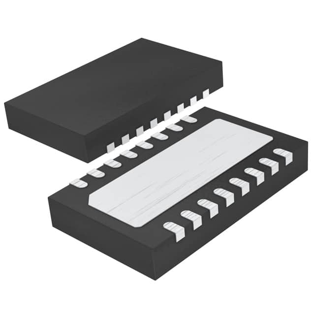
Analog Devices Inc. LTC4317CDHC#PBF
- Part No.:
- LTC4317CDHC#PBF
- Manufacturer:
- Analog Devices Inc.
- Category:
- Specialized
- Package:
- 16-WFDFN Exposed Pad
- Datasheet:
-
 LTC4317CDHC#PBF.pdf
- Description:
- IC INTERFACE SPECIALIZED 16DFN
- Quantity:
- Payment:

- Shipping:

Inventory:385
Please send an inquiry. Send us your inquiry, and we will respond immediately.
Product details
Overview
LTC4317CDHC#PBF from Analog Devices (formerly Linear Technology) is a dual-channel I²C/SMBus address translator IC that bridges master and slave bus segments to resolve hardwired address conflicts. It supports 2.25V–5.5V operation, provides ±4kV HBM ESD protection, enables resistor-configurable 7-bit address translation (up to 127 variants), and features automatic stuck-bus recovery and hot-swap capability for live board insertion. It is used in server backplanes and telecom chassis where multiple identical I²C sensors or PMBus devices share one bus.
For engineers reviewing the LTC4317CDHC#PBF datasheet, LTC4317CDHC#PBF pinout, LTC4317CDHC#PBF application, or LTC4317CDHC#PBF equivalent, key selection criteria include its dual-output channel architecture, pass-through mode via XORH pin, 400kHz I²C Fast Mode support, 16-lead DFN (5mm × 3mm) package with exposed GND pad, and resistor-based translation byte configuration without firmware involvement.
Technical Context
The LTC4317CDHC#PBF implements real-time 7-bit address translation using XOR logic between incoming SDAIN address bits and user-defined translation bytes set via analog voltage levels on XORL1/XORL2 (lower nibble) and XORH1/XORH2 (upper nibble). Each channel operates independently with dedicated READYn status outputs and ENABLEn controls.
Its internal hot-swap logic precharges SCL/SDA lines to 1V before enabling N1/N2 pass switches, preventing bus corruption during live insertion. Stuck-bus timeout (25–35ms) and glitch filtering (50–100ns) ensure robustness against abnormal conditions like premature STOP bits or low-hold faults.
Key Specifications
| Parameter | Value and Actual Design Meaning |
|---|---|
| Supply Voltage Range | 2.25V to 5.5V - supports level translation between 2.5V, 3.3V, and 5V I²C buses; VCC must connect to lower supply when interfacing mismatched voltages. |
| Max Clock Frequency | 400kHz - fully compatible with I²C Fast Mode, enabling high-speed sensor or power-management communication. |
| Address Translation | 7-bit XOR-based - enables up to 127 unique output addresses per channel using external resistive dividers on XORL/XORH pins; no software required. |
| Pass Switch RDS(ON) | 1.8Ω (at 5V), 2.2Ω (at 3.3V), 3Ω (at 2.25V) - ensures minimal signal degradation and voltage drop across SCL/SDA paths during translation. |
| Stuck Bus Timeout | 25–35ms - automatically reconnects SDAIN–SDAOUT if SCLIN remains static, preventing permanent bus lockup in noisy industrial environments. |
| ESD Rating | ±4kV HBM - protects against electrostatic discharge during handling and system integration in telecom and server assembly lines. |
| Operating Temp | 0°C to 70°C - commercial-grade temperature range suitable for controlled-environment applications like data center motherboard management. |
Pinout & Package
Package: 16-lead plastic DFN (5mm × 3mm) with exposed GND pad (Pin 17); RoHS-compliant, lead-free finish (PBF).
| Pin/Terminal | Circuit Role | Design Meaning |
|---|---|---|
| 1, 16 | GND | Device ground reference; exposed pad (Pin 17) is internally connected to GND and may be soldered to PCB ground plane for thermal and EMI performance. |
| 2, 3 | SCLOUT2, SCLOUT1 | Output-side clock lines for Slave Channel 2 and Channel 1; require external pull-up resistors to local bus supply voltage. |
| 4, 5 | SDAOUT1, SDAIN | Channel 1 output data line and shared input data line; SDAIN connects to master-side SDA; both require pull-up resistors. |
| 6, 7 | SDAOUT2, READY1 | Channel 2 output data line and ready-status open-drain output for Channel 1; READY1 pulls high when translation is configured and bus is idle. |
| 8, 9 | READY2, ENABLE2 | Ready-status output and enable input for Channel 2; ENABLE2 low disables translation and disconnects SDAIN–SDAOUT2 and SCLIN–SCLOUT2. |
| 10, 11 | XORH2, XORL2 | Upper and lower nibble configuration inputs for Channel 2 translation byte; DC voltage sets 3-bit (XORH2) and 4-bit (XORL2) portions of XOR mask. |
| 12, 13 | XORH1, XORL1 | Upper and lower nibble configuration inputs for Channel 1 translation byte; tied to resistive dividers between VCC and GND to set translation value. |
| 14, 15 | VCC, ENABLE1 | Power supply input (2.25–5.5V) and enable input for Channel 1; ENABLE1 rising edge triggers re-read of XORH1/XORL1 voltages and restarts configuration. |
Key Features
| Feature | Design Value |
|---|---|
| Dual independent channels | Enables two separate slave groups (e.g., temperature sensors on Channel 1, voltage monitors on Channel 2) to coexist on one master bus without address collision. |
| Resistor-configurable translation | Eliminates need for microcontroller firmware or EEPROM programming; translation byte set via precision 1% resistive dividers on XORL/XORH pins. |
| Pass-through mode | Asserting XORH1 or XORH2 high disables translation and maintains direct SCL/SDA connectivity - essential for general-call addressing (e.g., SMBus reset commands). |
| Hot-swap precharge | Internal 1V precharge (via 200kΩ) on SCLIN/SDAIN minimizes bus disturbance during live insertion, meeting I²C hot-swap requirements in modular telecom systems. |
| Stuck-bus auto-recovery | Monitors SCLIN for >30ms static state and forces bus reconnect, preventing system hang in environments with intermittent noise or faulty slaves. |
Applications
| Server Baseboard Management | Telecom Line Card Expansion |
|---|---|
|
Use Scenario: Multiple identical PMBus-compatible DC-DC converters installed across redundant server blades share one IPMI I²C bus. IC Role / Device Role / Timing Role: LTC4317CDHC#PBF acts as dual-channel address translator, assigning unique 7-bit addresses to each converter group to avoid arbitration failure. Use Value: Enables scalable BOM reuse without custom firmware or hardware redesign; supports hot-plug blade replacement without bus reset. |
Use Scenario: A central shelf controller communicates with identical optical transceivers across 16 line cards via a single backplane I²C bus. IC Role / Device Role / Timing Role: LTC4317CDHC#PBF bridges master bus to per-card slave buses, translating fixed 0x50 address to unique per-card offsets (e.g., 0x51–0x5F). Use Value: Eliminates need for discrete address jumpers or EEPROM programming on each card; reduces field service time and inventory SKUs. |
| Industrial Sensor Hub | Embedded System I²C Expansion |
|
Use Scenario: An MCU reads data from eight identical ambient light sensors mounted across different zones of a factory floor. IC Role / Device Role / Timing Role: LTC4317CDHC#PBF routes master SCL/SDA to two parallel sensor banks (four per channel), applying distinct XOR masks to assign non-overlapping addresses. Use Value: Achieves deterministic polling sequence and avoids bus contention; supports real-time fault isolation per sensor group. |
Use Scenario: A medical device mainboard integrates legacy I²C peripherals (EEPROM, RTC, ADC) with identical 0x68 addresses onto one interface. IC Role / Device Role / Timing Role: LTC4317CDHC#PBF serves as address expander, mapping each peripheral to a unique translated address (e.g., 0x69, 0x6A, 0x6B) while preserving timing compliance. Use Value: Avoids costly redesign of legacy components; maintains full I²C Fast Mode throughput without introducing protocol-level latency. |
Equivalent & Alternatives
The following parts are listed as comparable options for similar I²C address translation applications.
| Alternative Part | Technical Difference | Application Difference | Selection Advice |
|---|---|---|---|
| LTC4302-2 | Software-configurable 2-wire buffer with GPIO and addressable enable; requires I²C command writes to set address map; no resistor-based translation. | Used where dynamic reconfiguration is needed (e.g., field-upgradable systems); lacks pass-through mode and hot-swap precharge. | Select LTC4302-2 only if firmware control of address mapping is required; LTC4317CDHC#PBF is preferred for zero-software, hardware-only deployment. |
| LTC4305 | 2-channel I²C multiplexer with capacitance buffering and fault reporting; routes master to one of two downstream buses but does not translate addresses. | Suitable for bus segmentation where slaves have unique addresses already; cannot resolve same-address conflicts on a single downstream bus. | Choose LTC4305 when isolation and fault containment are primary; LTC4317CDHC#PBF is necessary when multiple identical slaves must share one physical bus segment. |
Compared with LTC4302-2 and LTC4305, the LTC4317CDHC#PBF uniquely delivers hardware-only, resistor-configured address translation with built-in hot-swap safety and pass-through mode - making it optimal for cost-sensitive, firmware-constrained systems requiring deterministic, maintenance-free I²C expansion.
Availability
LTC4317CDHC#PBF is available at Aetrix Electronics and suitable for server baseboard management, telecom line card expansion, and industrial sensor hub applications requiring stable component supply, long-term lifecycle support, and RoHS-compliant packaging.
Supply support for LTC4317CDHC#PBF includes scheduled delivery planning, volume procurement assistance, BOM continuity management, traceable sourcing, and lifecycle availability coordination for OEM customers, industrial embedded developers, connected-device designers, and electronics production programs.
Manufacturer
Analog Devices acquired Linear Technology in 2017 and maintains full technical and manufacturing continuity for all Linear IC products, including precision analog, power management, and interface solutions.
The LTC4317CDHC#PBF belongs to Linear's I²C/SMBus infrastructure portfolio, designed specifically to solve address collision and hot-swap challenges in dense, modular electronic systems such as data center servers and carrier-grade networking equipment.
FAQ
What is the function of the XORH and XORL pins on the LTC4317CDHC#PBF?
The XORH1/XORH2 and XORL1/XORL2 pins on the LTC4317CDHC#PBF configure the 7-bit address translation byte: XORH sets the upper 3 bits and XORL sets the lower 4 bits via analog voltage levels generated by external resistive dividers. When XORH is pulled high, the LTC4317CDHC#PBF enters pass-through mode, disabling translation and connecting input/output buses directly. This hardware-based configuration eliminates firmware dependencies and enables field-programmable addressing without reprogramming.
Does the LTC4317CDHC#PBF support I²C Fast Mode Plus (1MHz)?
No, the LTC4317CDHC#PBF supports up to 400kHz I²C Fast Mode, as specified in its Electrical Characteristics table under fSCL(MAX). It does not meet the timing or drive-strength requirements for Fast Mode Plus (1MHz). For systems requiring >400kHz operation, alternative solutions such as dedicated high-speed multiplexers or FPGA-based bridging must be considered - the LTC4317CDHC#PBF is optimized for robustness and address resolution, not maximum speed.
How does the LTC4317CDHC#PBF handle hot-swap insertion into an active I²C bus?
The LTC4317CDHC#PBF uses internal precharge circuitry to set SCLIN and SDAIN lines to 1V through 200kΩ resistors before enabling pass switches N1 and N2. This prevents bus glitches or false START/STOP detection during live insertion. The device waits for bus idle (≥120µs high state or STOP bit) and ENABLE high before asserting READYn and connecting the buses. This sequence ensures zero disruption to ongoing I²C transactions on the master side - a critical feature for telecom and server hot-swap architectures.
Can the LTC4317CDHC#PBF translate 10-bit I²C addresses?
No, the LTC4317CDHC#PBF is explicitly designed for 7-bit I²C/SMBus addressing and does not support 10-bit addressing protocols. Its translation logic operates exclusively on the 7-bit address portion of the I²C frame, and the datasheet lists "10-Bit Addressing" under Unsupported I²C Protocols. Attempting to use it with 10-bit devices will result in incorrect or failed communication - design validation must confirm all connected slaves use standard 7-bit addressing.
What is the purpose of the READY1 and READY2 pins on the LTC4317CDHC#PBF?
READY1 and READY2 are open-drain status outputs indicating successful configuration and bus readiness per channel. Each pin goes high (when pulled up externally) after the LTC4317CDHC#PBF reads XORH/XORL voltages, confirms bus idle, and enables N1/N2 pass switches - signaling that address translation is active and the channel is safe for master communication. They provide hardware handshaking for system boot sequences and fault diagnostics, eliminating reliance on software polling or timeout-based initialization.
LTC4317CDHC#PBF Specifications
- Product attributes
- Attribute value
- Manufacturer:
- Analog Devices Inc.
- Series:
- -
- Package/Case:
- 16-WFDFN Exposed Pad
- Packaging:
- Tube
- Product Status:
- Active
- Applications:
- Address Translator
- Interface:
- I2C
- Voltage - Supply:
- 2.25V ~ 5.5V
- Supplier Device Package:
- 16-DFN (5x3)
- Grade:
- -
- Qualification:
- -
- Mounting Type:
- Surface Mount
LTC4317CDHC#PBF FAQ
1.How can I place an order for LTC4317CDHC#PBF through Aetrix?
Please submit a Request for Quotation (RFQ) for LTC4317CDHC#PBF on Aetrix. Our sales agent will provide a competitive quotation and guide you through the order confirmation once you accept the terms.
2.Are the price and stock information for LTC4317CDHC#PBF reliable?
The price and inventory of LTC4317CDHC#PBF are updated periodically and may fluctuate due to market conditions. Stock and pricing data are typically refreshed every 24 hours. Quotation validity for LTC4317CDHC#PBF is usually 5 days.
3.What payment methods are accepted for LTC4317CDHC#PBF?
We accept Wire Transfer, PayPal, Credit Card, Western Union, MoneyGram, and Escrow for LTC4317CDHC#PBF transactions.
Note: Certain payment methods may incur a processing fee.
4.How is shipping managed for LTC4317CDHC#PBF?
LTC4317CDHC#PBF orders can be shipped via leading logistics carriers, including DHL, UPS, FedEx, TNT, or Registered Mail.
Once your LTC4317CDHC#PBF order is processed, you will receive an email with the shipment details and tracking number.
Note: Tracking information may take up to 24 hours to appear. Express delivery typically takes 3–5 business days.
5.How can I obtain technical support or documentation for LTC4317CDHC#PBF?
For technical support, including LTC4317CDHC#PBF datasheets, pinout diagrams, or application guidance, please contact our engineering support team. They can provide detailed documentation and assistance for your LTC4317CDHC#PBF requirements.
6.How does Aetrix verify that LTC4317CDHC#PBF is sourced from the original manufacturer or authorized distributors?
All LTC4317CDHC#PBF products on Aetrix are procured from qualified distributors and authorized channels. Our dedicated quality assurance team conducts strict verification, including traceability checks and, if necessary, third-party testing. This ensures that LTC4317CDHC#PBF meets industry standards.
7.What is the process for return or replacement of LTC4317CDHC#PBF?
All LTC4317CDHC#PBF units undergo pre-shipment inspection (PSI). If there is an issue with LTC4317CDHC#PBF, returns or replacements are accepted under the following conditions:
1.Quantity discrepancies, incorrect items, or visible external defects (such as breakage or corrosion), acknowledged by Aetrix.
2.The issue is reported within 90 days of delivery.
3.The LTC4317CDHC#PBF part is unused and in its original packaging.
Return procedure for LTC4317CDHC#PBF:
1.Submit a request within 90 days.
2.Obtain a Return Material Authorization (RMA) from Aetrix.
LTC4317CDHC#PBF Tags

-
NVT4857UKAZ
NXP Semiconductors

-
TCA8418RTWR
Texas Instruments

-
PCA9546APWR
Texas Instruments

-
MD0100N8-G
Microchip Technology

-
PCA9548APW,118
NXP Semiconductors

-
PCA9540BDP,118
NXP Semiconductors

-
PCA9548APWR
Texas Instruments

-
PCA9546APW,118
NXP Semiconductors

-
PTN3360DBS,518
NXP Semiconductors

-
PCA9546ABS,118
NXP Semiconductors

-
PCA9518PWR
Texas Instruments

-
PCA9545APW,118
NXP Semiconductors
Tech Hub

A practical engineering guide to 3.3V and 5V logic compatibility, input thresholds, resistor dividers, translator ICs, MOSFET level shifting, I2C pull-ups, timing limits and power-sequencing risks.

The 74HC595 uses push-pull logic outputs, while the TPIC6B595 uses 50 V open-drain DMOS sinks for higher-power loads. This guide compares timing, current limits, 3.3 V interfacing, load wiring, thermal…

The 74HC595 converts serial data into eight stable parallel outputs. This guide covers pin functions, shift and storage timing, OE and MR behavior, drive-current limits, cascading, voltage compatibilit…

A technical comparison of level-sensitive latches and edge-triggered flip-flops, covering timing windows, setup and hold limits, master–slave operation, time borrowing, race-through, HDL inference and…

A D latch stores one bit while Enable controls when data can pass. This reference covers gate-level operation, truth tables, transparency, setup and hold timing, LE versus OE, common ICs and practical …

An SR latch stores one bit through cross-coupled feedback. This engineering reference covers NOR and NAND implementations, truth tables, forbidden-state recovery, gated operation, switch debouncing, fa…

Latch circuits retain one bit through feedback. This technical reference covers SR and D latches, truth tables, transparency, timing limits, latch-versus-flip-flop behavior, applications and common log…

An engineering guide to LED driver operation, constant-current and constant-voltage outputs, linear and switching topologies, dimming, IC selection, calculations, replacement compatibility, and fault c…

Operational amplifier guide covering op amp basics, feedback, ideal vs real op amps, common configurations, buffer circuits, offset, bias current, gain-bandwidth, slew rate, rail-to-rail limits and sel…

Jumper cables guide covering safe connection order, red and black clamp placement, final ground connection, cable gauge, length, clamp quality, copper vs CCA cables, jump starter comparison and battery…


