
 My Inquiry
 My Account


Analog Devices Inc. LTC6563IUDDM#PBF
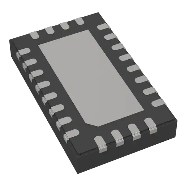
- Part No.:
- LTC6563IUDDM#PBF
- Manufacturer:
- Analog Devices Inc.
- Category:
- Special Purpose Amplifiers
- Package:
- 24-WFQFN Exposed Pad
- Datasheet:
-
 LTC6563IUDDM#PBF.pdf
- Description:
- QUAD CHANNEL TRANSIMPEDANCE AMPL
- Quantity:
- Payment:

- Shipping:

Inventory:1,483
Please send an inquiry. Send us your inquiry, and we will respond immediately.
Product details
Overview
LTC6563IUDDM#PBF from Analog Devices is a four-channel transimpedance amplifier (TIA) optimized for LIDAR receiver front-ends using avalanche photodiodes (APDs) or photodiodes (PDs). It delivers 600MHz –3dB bandwidth with 0.5pF input capacitance, selectable transimpedance gains of 5.55/11.1/16.7/22.2kΩ, and 90µA linear input current range - enabling high-speed, low-noise optical signal conversion in automotive and industrial LIDAR systems.
For engineers reviewing the LTC6563IUDDM#PBF datasheet, LTC6563IUDDM#PBF pinout, LTC6563IUDDM#PBF application, or LTC6563IUDDM#PBF equivalent, key selection criteria include its integrated 4:1 output MUX, fast 10ns channel switching, differential 2VP-P swing into 100Ω, 2.5ns overload recovery, and AEC-Q100 Grade 1 qualification for automotive LIDAR deployment.
Technical Context
The LTC6563IUDDM#PBF integrates four independent TIAs with programmable gain via ADJ0/ADJ1 pins, each supporting DC-coupled APD/PD inputs and featuring internal offset cancellation (OFFSET pin), common-mode control (CM pin), and tilt adjustment (TILT pin) for dynamic output shaping. Its architecture enables precise current-to-voltage conversion while maintaining linearity across –40°C to +85°C.
Channel selection is managed by CHSEL0/CHSEL1, with OMUX controlling internal 4:1 multiplexing; PWRMD enables shutdown mode (13mW total power). The device drives differential ADC inputs directly via OUT/OUT outputs with built-in 100Ω termination (TERM/TERM), eliminating external components for 100Ω differential loads.
Key Specifications
| Parameter | Value and Actual Design Meaning |
|---|---|
| –3dB Bandwidth | 600MHz at 0.5pF input capacitance - supports sub-nanosecond pulse detection in time-of-flight LIDAR. |
| Transimpedance Gain | Selectable 5.55/11.1/16.7/22.2kΩ - matches varying APD responsivity and dynamic range requirements. |
| Input Current Noise Density | 1.8pA/√Hz @ 100MHz, 3.7pA/√Hz @ 600MHz (0.5pF) - enables high SNR in low-light LIDAR operation. |
| Differential Output Swing | Up to 2VP-P into 100Ω load - directly interfaces with high-speed ADCs like AD9094 without external amplification. |
| Channel Switching Time | 10ns between any channels - critical for multi-zone scanning LIDAR with rapid beam steering. |
| Overload Recovery | 2.5ns recovery from >1A transient input - maintains timing integrity after strong ambient light or sun exposure events. |
| Supply Voltage | 3.15V to 3.45V (3.3V nominal) on both VCCI and VCCO rails - ensures stable operation under automotive voltage fluctuations. |
| Operating Temperature | –40°C to +85°C - qualified per AEC-Q100 Grade 1 for under-hood automotive LIDAR applications. |
Pinout & Package
The LTC6563IUDDM#PBF is housed in a 3mm × 5mm, 24-pin QFN package with exposed thermal pad (Pin 25 = GND) and wettable flanks for automated optical inspection (AOI). Pin numbering follows standard top-view orientation with Pin 1 at top-left corner.
| Pin/Terminal | Circuit Role | Design Meaning |
|---|---|---|
| IN1–IN4 | Photodiode input terminals | Four independent, DC-coupled TIA inputs accepting APD/PD anode/cathode configurations. |
| OUT / OUT | Differential output pair | High-speed complementary outputs delivering 2VP-P swing into 100Ω; routed to ADC inputs. |
| TERM / TERM | Internal termination connection points | Internally tied to 100Ω differential termination; must be connected to OUT/OUT for proper impedance matching. |
| CHSEL0 / CHSEL1 | Channel select control inputs | Binary-encoded selection of active TIA channel (00–11); enable sequential or random access scanning. |
| OMUX | Multiplexer enable | Logic-high enables internal 4:1 MUX; logic-low disables MUX and outputs all four channels simultaneously. |
| PWRMD | Power-down control | Logic-low places device in shutdown mode (6.3mA total supply current), reducing system power during idle periods. |
| CM | Common-mode voltage control | Analog input setting differential output common-mode level (0.38V–2.3V range) for ADC input alignment. |
| OFFSET | Input current cancellation | Adjusts input offset current up to ±240µA to null dark current or bias drift in APD arrays. |
| TILT | Differential output slope control | Programs output gain slope (–1.25 to –0.7 V/V) to compensate for photodiode nonlinearity or signal path loss. |
| HI | Output clamping reference | Sets upper clamp voltage for differential output; must exceed CM pin voltage by ≥0.2V to avoid clipping. |
| VCCI / VCCO | Independent supply rails | VCCI powers input stage; VCCO powers output stage - enables PSRR optimization and noise isolation. |
| GND (Pins 1, 3, 5, 7, 11, 13, 15, 25) | Ground connections | Eight dedicated GND pins including exposed pad (Pin 25) - minimize ground bounce and improve thermal dissipation. |
Key Features
| Feature | Design Value |
|---|---|
| Integrated 4:1 output MUX | Reduces PCB routing complexity and ADC channel count by multiplexing four TIAs onto one differential pair. |
| External channel expansion support | Enables up to 64-channel systems using multiple LTC6563IUDDM#PBF devices - ideal for high-resolution solid-state LIDAR. |
| Programmable transimpedance gain | Four discrete RT values (5.55–22.2kΩ) selected via ADJ0/ADJ1 pins - eliminates external feedback resistors and improves layout flexibility. |
| Fast overload recovery (2.5ns) | Preserves timing accuracy after saturation events (e.g., sunlight glare), avoiding dead-time penalties in pulsed LIDAR. |
| AEC-Q100 Grade 1 qualification | Validated for automotive use from –40°C to +125°C junction temperature - meets stringent reliability requirements for ADAS sensors. |
| Wettable flank QFN package | Supports automated optical inspection (AOI) of solder joints - critical for high-yield manufacturing of safety-critical LIDAR modules. |
Applications
| Automotive LIDAR Receiver | Industrial LIDAR Receiver |
|---|---|
|
Use Scenario: Front-facing long-range LIDAR in autonomous vehicles detecting objects beyond 200m under variable lighting. IC Role / Device Role / Timing Role: Four-channel TIA converting APD photocurrents into amplified, multiplexed differential voltage signals synchronized to laser pulse timing. Use Value: 600MHz bandwidth and 2.5ns overload recovery ensure accurate time-of-flight measurement even during solar interference events. |
Use Scenario: Warehouse robotic navigation using short-range flash LIDAR for obstacle avoidance and SLAM mapping. IC Role / Device Role / Timing Role: High-linearity TIA front-end digitizing multi-pixel photodiode array outputs with minimal distortion across 0–90µA input range. Use Value: Selectable 5.55–22.2kΩ gain allows optimal SNR tuning for varying reflectivity surfaces (e.g., black plastic vs. white wall). |
| Multi-Zone Scanning LIDAR | High-Speed Optical Time-Domain Reflectometry |
|
Use Scenario: Rotating or MEMS-based LIDAR scanning 32+ angular zones per revolution with real-time channel switching. IC Role / Device Role / Timing Role: Channel-selectable TIA providing 10ns inter-channel transition for seamless zone-to-zone signal acquisition. Use Value: Internal 4:1 MUX and external daisy-chain capability reduce system-level component count and power consumption by >40% vs. discrete solutions. |
Use Scenario: Fiber-optic fault location in telecom infrastructure requiring picosecond-level pulse response fidelity. IC Role / Device Role / Timing Role: Ultra-low-noise TIA capturing weak backscattered optical pulses with 1.8pA/√Hz input noise density at 100MHz. Use Value: 65nARMS integrated input-referred noise over 600MHz bandwidth enables detection of sub-millimeter fiber discontinuities. |
Equivalent & Alternatives
The following parts are listed as comparable options for similar transimpedance amplifier applications.
| Alternative Part | Technical Difference | Application Difference | Selection Advice |
|---|---|---|---|
| MAX40660ATB/VY+ | Single-channel 650MHz TIA with 1.2pA/√Hz noise; no integrated MUX or channel selection logic. | Requires external multiplexing for multi-channel systems; better suited for compact single-zone receivers. | Choose when board space is constrained and only one APD channel is needed per IC. |
| ADN3010-11 | 11.3Gbps limiting amplifier with integrated TIA; fixed 50Ω input impedance and no programmable gain. | Targeted at telecom datacom (not LIDAR); lacks overload recovery spec and automotive qualification. | Consider only for high-speed serial optical links - not suitable for pulsed LIDAR waveform capture. |
Compared with MAX40660ATB/VY+ and ADN3010-11, the LTC6563IUDDM#PBF uniquely combines quad-channel integration, programmable gain, internal MUX, AEC-Q100 qualification, and LIDAR-optimized overload recovery - making it the only drop-in solution for scalable, automotive-grade multi-zone LIDAR front-ends.
Availability
LTC6563IUDDM#PBF is available at Aetrix Electronics and suitable for automotive LIDAR receiver, industrial LIDAR receiver, and multi-zone scanning LIDAR applications requiring stable component supply, long-term lifecycle support, and AEC-Q100-compliant sourcing.
Supply support for LTC6563IUDDM#PBF includes scheduled delivery planning, volume procurement assistance, BOM continuity management, traceable sourcing, and lifecycle availability coordination for OEM customers, industrial embedded developers, connected-device designers, and electronics production programs.
Manufacturer
Analog Devices, Inc. is a global leader in high-performance analog, mixed-signal, and digital signal processing semiconductors, serving precision instrumentation, industrial automation, and automotive safety markets.
The LTC6563IUDDM#PBF belongs to Analog Devices' LIDAR signal chain portfolio, designed specifically to address the low-noise, high-bandwidth, and automotive reliability demands of next-generation optical sensing systems.
FAQ
What is the maximum input capacitance supported by the LTC6563IUDDM#PBF while maintaining 600MHz bandwidth?
The LTC6563IUDDM#PBF achieves its full 600MHz –3dB bandwidth with a total input capacitance (CIN,TOT) of 0.5pF, as specified in the AC Electrical Characteristics table. Performance degrades with higher capacitance: at 2pF, bandwidth drops to ~450MHz; at 4pF, it falls to ~300MHz. For optimal LIDAR pulse fidelity, APD selection and PCB layout must keep total node capacitance ≤0.5pF.
How does the OFFSET pin function in the LTC6563IUDDM#PBF, and what is its cancellation range?
The OFFSET pin on the LTC6563IUDDM#PBF provides programmable input current cancellation to null APD dark current or sensor bias drift. Applying 0V to 3.3V generates a cancellation current from 0µA to 240µA (typical), with transconductance of –110µA/V (typical). This feature enables DC stabilization of the TIA input without external op-amps or complex calibration circuits.
Can the LTC6563IUDDM#PBF drive a 50Ω single-ended ADC input, or is it strictly for 100Ω differential loads?
The LTC6563IUDDM#PBF is optimized for 100Ω differential loads via its OUT/OUT outputs and internal TERM/TERM termination. While it can drive 50Ω single-ended loads (achieving 2.4VP-P swing with center-grounded 75Ω per side), doing so requires external termination and forfeits common-mode rejection. For best noise immunity and timing accuracy, use the differential 100Ω configuration as intended.
What is the purpose of the HI pin on the LTC6563IUDDM#PBF, and how should it be configured?
The HI pin on the LTC6563IUDDM#PBF sets the upper clamp voltage for the differential output stage. It must be biased ≥0.2V above the CM pin voltage to prevent clipping. Default HI voltage is 1.8V; adjusting it allows fine-tuning of output headroom - especially useful when interfacing with ADCs having specific input voltage limits or when compensating for PCB trace losses.
Is the LTC6563IUDDM#PBF pin-compatible with other variants in the LTC656x family, such as the LTC6560 or LTC6561?
No, the LTC6563IUDDM#PBF is not pin-compatible with the LTC6560 or LTC6561. It uses a unique 24-pin QFN (UDDM) package with distinct pin assignments for OMUX, TILT, and OFFSET functions absent in earlier variants. Migration requires PCB redesign; however, functional overlap exists in transimpedance gain range and bandwidth, enabling schematic-level reuse with layout adaptation.
LTC6563IUDDM#PBF Specifications
- Product attributes
- Attribute value
- Manufacturer:
- Analog Devices Inc.
- Series:
- -
- Package/Case:
- 24-WFQFN Exposed Pad
- Packaging:
- Tube
- Product Status:
- Active
- Type:
- Transimpedance Amplifier
- Applications:
- Receiver
- Mounting Type:
- Surface Mount, Wettable Flank
- Grade:
- -
- Qualification:
- -
- Supplier Device Package:
- 24-QFN (3x5)
LTC6563IUDDM#PBF FAQ
1.How can I place an order for LTC6563IUDDM#PBF through Aetrix?
Please submit a Request for Quotation (RFQ) for LTC6563IUDDM#PBF on Aetrix. Our sales agent will provide a competitive quotation and guide you through the order confirmation once you accept the terms.
2.Are the price and stock information for LTC6563IUDDM#PBF reliable?
The price and inventory of LTC6563IUDDM#PBF are updated periodically and may fluctuate due to market conditions. Stock and pricing data are typically refreshed every 24 hours. Quotation validity for LTC6563IUDDM#PBF is usually 5 days.
3.What payment methods are accepted for LTC6563IUDDM#PBF?
We accept Wire Transfer, PayPal, Credit Card, Western Union, MoneyGram, and Escrow for LTC6563IUDDM#PBF transactions.
Note: Certain payment methods may incur a processing fee.
4.How is shipping managed for LTC6563IUDDM#PBF?
LTC6563IUDDM#PBF orders can be shipped via leading logistics carriers, including DHL, UPS, FedEx, TNT, or Registered Mail.
Once your LTC6563IUDDM#PBF order is processed, you will receive an email with the shipment details and tracking number.
Note: Tracking information may take up to 24 hours to appear. Express delivery typically takes 3–5 business days.
5.How can I obtain technical support or documentation for LTC6563IUDDM#PBF?
For technical support, including LTC6563IUDDM#PBF datasheets, pinout diagrams, or application guidance, please contact our engineering support team. They can provide detailed documentation and assistance for your LTC6563IUDDM#PBF requirements.
6.How does Aetrix verify that LTC6563IUDDM#PBF is sourced from the original manufacturer or authorized distributors?
All LTC6563IUDDM#PBF products on Aetrix are procured from qualified distributors and authorized channels. Our dedicated quality assurance team conducts strict verification, including traceability checks and, if necessary, third-party testing. This ensures that LTC6563IUDDM#PBF meets industry standards.
7.What is the process for return or replacement of LTC6563IUDDM#PBF?
All LTC6563IUDDM#PBF units undergo pre-shipment inspection (PSI). If there is an issue with LTC6563IUDDM#PBF, returns or replacements are accepted under the following conditions:
1.Quantity discrepancies, incorrect items, or visible external defects (such as breakage or corrosion), acknowledged by Aetrix.
2.The issue is reported within 90 days of delivery.
3.The LTC6563IUDDM#PBF part is unused and in its original packaging.
Return procedure for LTC6563IUDDM#PBF:
1.Submit a request within 90 days.
2.Obtain a Return Material Authorization (RMA) from Aetrix.
LTC6563IUDDM#PBF Tags

-
TSM103WIDT
STMicroelectronics

-
LM392M/NOPB
Texas Instruments
-
MCP6S93T-E/UN
Microchip Technology
-
INA137UA/2K5
Texas Instruments
-
INA134UA/2K5
Texas Instruments
-
TS34118CS28 RDG
Taiwan Semiconductor Corporation

-
SI8920BC-IPR
Skyworks Solutions Inc.
-
ADUM3190ARQZ-RL7
Analog Devices Inc.
-
ADUM3190ARQZ
Analog Devices Inc.
-
AMC1311BDWVR
Texas Instruments
-
AMC1350DWVR
Texas Instruments
-
ADUM3190SRQZ-RL7
Analog Devices Inc.
Tech Hub

A practical engineering guide to 3.3V and 5V logic compatibility, input thresholds, resistor dividers, translator ICs, MOSFET level shifting, I2C pull-ups, timing limits and power-sequencing risks.

The 74HC595 uses push-pull logic outputs, while the TPIC6B595 uses 50 V open-drain DMOS sinks for higher-power loads. This guide compares timing, current limits, 3.3 V interfacing, load wiring, thermal…

The 74HC595 converts serial data into eight stable parallel outputs. This guide covers pin functions, shift and storage timing, OE and MR behavior, drive-current limits, cascading, voltage compatibilit…

A technical comparison of level-sensitive latches and edge-triggered flip-flops, covering timing windows, setup and hold limits, master–slave operation, time borrowing, race-through, HDL inference and…

A D latch stores one bit while Enable controls when data can pass. This reference covers gate-level operation, truth tables, transparency, setup and hold timing, LE versus OE, common ICs and practical …

An SR latch stores one bit through cross-coupled feedback. This engineering reference covers NOR and NAND implementations, truth tables, forbidden-state recovery, gated operation, switch debouncing, fa…

Latch circuits retain one bit through feedback. This technical reference covers SR and D latches, truth tables, transparency, timing limits, latch-versus-flip-flop behavior, applications and common log…

An engineering guide to LED driver operation, constant-current and constant-voltage outputs, linear and switching topologies, dimming, IC selection, calculations, replacement compatibility, and fault c…

Operational amplifier guide covering op amp basics, feedback, ideal vs real op amps, common configurations, buffer circuits, offset, bias current, gain-bandwidth, slew rate, rail-to-rail limits and sel…

Jumper cables guide covering safe connection order, red and black clamp placement, final ground connection, cable gauge, length, clamp quality, copper vs CCA cables, jump starter comparison and battery…


