
 My Inquiry
 My Account


Analog Devices Inc. LTC6652BHLS8-5
- Part No.:
- LTC6652BHLS8-5
- Manufacturer:
- Analog Devices Inc.
- Category:
- Voltage Reference
- Package:
- 8-CLCC
- Datasheet:
-
 LTC6652BHLS8-5.pdf
- Description:
- IC VREF SERIES 0.1% 8LCC
- Quantity:
- Payment:

- Shipping:

Inventory:4,910
Please send an inquiry. Send us your inquiry, and we will respond immediately.
Product details
Overview
LTC6652BHLS8-5 from Analog Devices (acquired Linear Technology) is a precision buffered voltage reference IC delivering 5.000 V output with ±0.1% initial accuracy, 8 ppm/°C max temperature coefficient (B-grade, LS8 package), and 2.8 ppmP-P (0.1 Hz–10 Hz) low-frequency noise. It operates from 2.7 V to 13.2 V supply, sinks/sources ±5 mA, and is specified over –40°C to 125°C for automotive sensor signal conditioning and high-resolution ADC biasing.
For engineers reviewing the LTC6652BHLS8-5 datasheet, LTC6652BHLS8-5 pinout, LTC6652BHLS8-5 application, or LTC6652BHLS8-5 equivalent, key selection criteria include hermetic LS8 package stability, thermal hysteresis ≤45 ppm (–40°C to 125°C), long-term drift of 20 ppm/√kHr, shutdown current <2 µA, and guaranteed 5 mA sourcing/sinking capability at 5 V output.
Technical Context
The LTC6652BHLS8-5 employs high-order curvature-compensated bandgap architecture to achieve predictable, monotonic temperature behavior and low drift. Its internal buffered output eliminates load regulation sensitivity-maintaining ≤75 ppm/mA sourcing and ≤450 ppm/mA sinking error across full temperature range.
It integrates active shutdown control with hysteresis on SHDN input (VTH_UP ≈ 2.0 V, VTH_DN ≈ 1.5 V), enabling robust low-power operation in battery-backed systems. The LS8 ceramic LCC package provides hermetic sealing, eliminating humidity-induced drift and supporting stable performance in harsh industrial environments.
Key Specifications
| Parameter | Value and Actual Design Meaning |
|---|---|
| Output Voltage | 5.000 V ±0.1% - tight initial tolerance enables 16-bit+ ADC calibration without trimming. |
| Temp Coefficient | 8 ppm/°C max (–40°C to 125°C) - B-grade spec for LS8 package ensures predictable drift in automotive under-hood applications. |
| Low-Freq Noise | 2.8 ppmP-P (0.1 Hz–10 Hz) - ultra-low flicker noise critical for precision weigh scales and strain gauge bridges. |
| Load Drive | ±5 mA sourcing/sinking - sufficient to drive SAR ADC reference inputs and op-amp bias networks directly. |
| Shutdown Current | <2 µA - enables microamp-level power budgeting in always-on sensor nodes. |
| Long-Term Drift | 20 ppm/√kHr - quantified reliability metric for 10+ year field deployments in medical instrumentation. |
| Thermal Hysteresis | 45 ppm (–40°C ↔ 125°C) - hermetic LS8 package minimizes mechanical stress memory effects. |
Pinout & Package
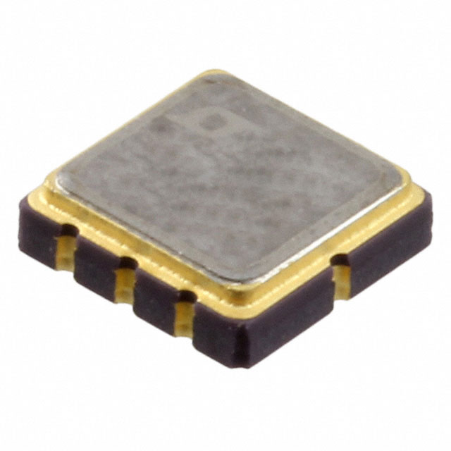
The LTC6652BHLS8-5 uses an 8-pin leadless ceramic chip carrier (LCC), 5 mm × 5 mm, hermetically sealed (LS8 package). Pins are arranged in a square configuration with exposed ground paddle; all GND pins must be soldered to PCB ground plane for thermal and electrical stability.
| Pin/Terminal | Circuit Role | Design Meaning |
|---|---|---|
| DNC (Pin 1) | Do Not Connect | No internal connection; must remain floating per datasheet to avoid parasitic coupling. |
| VIN (Pin 2) | Power Input | Accepts 2.7 V–13.2 V; requires local 0.1 µF bypass to GND for optimal PSRR above 10 kHz. |
| SHDN (Pin 3) | Active-Low Enable | Logic low (<1.5 V) disables output and reduces current to <2 µA; tie to VIN for normal operation. |
| GND (Pin 4) | Main Ground Reference | Primary return path; connects internally to die substrate and must be low-impedance. |
| GND (Pins 5,7,8) | Supplementary Grounds | Internally tied to Pin 4; all must be connected to PCB ground plane to minimize thermal gradient and noise. |
| VOUT (Pin 6) | Regulated Output | 5.000 V buffered source/sink node; stable without external capacitor but benefits from 0.1–10 µF for transient immunity. |
Key Features
| Feature | Design Value |
|---|---|
| Hermetic LS8 Packaging | Eliminates humidity-induced drift and enables stable operation in high-moisture industrial enclosures. |
| Guaranteed ±5 mA Drive | Supports direct interface to high-capacitance ADC reference inputs and multi-op-amp bias networks without external buffers. |
| Curvature-Compensated Bandgap | Delivers monotonic, predictable temperature response-critical for closed-loop calibration algorithms. |
| Low Dropout (300 mV) | Enables operation from low headroom supplies (e.g., 5.3 V rail powering 5 V reference) without sacrificing accuracy. |
| 100% Temp Testing | Every unit tested at –40°C, +25°C, and +125°C ensures guaranteed specs across full automotive grade range. |
Applications
| Automotive Engine Control Unit (ECU) | High-Resolution Industrial DAQ |
|---|---|
Use Scenario: Precision analog front-end for cylinder pressure sensors and wideband O2 sensors operating at 125°C under hood. IC Role / Device Role / Timing Role: Primary 5 V reference for 24-bit sigma-delta ADCs digitizing sensor outputs. Use Value: 8 ppm/°C drift and 45 ppm thermal hysteresis ensure <±0.01% total error over thermal cycling-meeting ASIL-B functional safety margin. | Use Scenario: Multi-channel data acquisition system measuring strain, temperature, and vibration in factory-floor machinery. IC Role / Device Role / Timing Role: Shared reference for simultaneous-sampling ADCs across 8 channels. Use Value: ±5 mA sourcing/sinking and 2.8 ppmP-P noise enable 120 dB SNR at 1 kSPS without external filtering. |
| Medical Patient Monitor | Test & Measurement Equipment |
Use Scenario: ECG/EEG analog signal chain requiring stable DC bias and low-noise excitation in portable battery-powered units. IC Role / Device Role / Timing Role: Low-power 5 V reference for instrumentation amplifiers and anti-alias filters. Use Value: <2 µA shutdown current extends battery life; hermetic LS8 prevents calibration drift during sterilization cycles. | Use Scenario: Benchtop multimeter and calibrator requiring traceable, stable reference for autoranging and self-test functions. IC Role / Device Role / Timing Role: Primary 5 V reference for internal DAC-based voltage generation and ADC linearity verification. Use Value: 20 ppm/√kHr long-term drift and 0.1% initial accuracy support annual recalibration intervals without interpolation uncertainty. |
Equivalent & Alternatives
The following parts are listed as comparable options for similar precision voltage reference applications.
| Alternative Part | Technical Difference | Application Difference | Selection Advice |
|---|---|---|---|
| REF5050IDR | 5 V, 3 ppm/°C max, SOIC-8, non-hermetic plastic package; higher PSRR but no shutdown. | Suitable for lab-grade instruments where ambient humidity is controlled; not rated for automotive temp range. | Select when lower drift is prioritized over shutdown capability and hermeticity. |
| ADR4550BRZ | 5 V, 3 ppm/°C max, SOIC-8, hermetic metal can; no shutdown; 1.8 µA quiescent current. | Used in aerospace avionics where radiation tolerance and long-term stability dominate; lacks LS8's thermal hysteresis advantage. | Select for ultra-stable, zero-shutdown applications where board space allows larger SOIC footprint. |
Compared with REF5050IDR and ADR4550BRZ, the LTC6652BHLS8-5 uniquely combines automotive-grade temperature range, integrated shutdown, hermetic LS8 packaging, and guaranteed ±5 mA drive-making it optimal for space-constrained, high-reliability embedded systems requiring both precision and power management.
Availability
LTC6652BHLS8-5 is available at Aetrix Electronics and suitable for automotive engine control, industrial data acquisition, and medical patient monitoring requiring stable component supply across extended temperature ranges and long product lifecycles.
Supply support for LTC6652BHLS8-5 includes scheduled delivery planning, volume procurement assistance, BOM continuity management, traceable sourcing, and lifecycle availability coordination for OEM customers, industrial embedded developers, connected-device designers, and electronics production programs.
Manufacturer
Analog Devices, Inc. (ADI) acquired Linear Technology in 2017 and maintains its precision analog portfolio, including voltage references, with focus on high-performance, high-reliability signal chain components.
The LTC6652 family was designed specifically for demanding applications requiring low drift, low noise, and robust operation across –40°C to 125°C-targeting automotive, industrial, and medical instrumentation markets.
FAQ
What is the maximum supply voltage for the LTC6652BHLS8-5?
The LTC6652BHLS8-5 supports a maximum input voltage of 13.2 V. Exceeding this rating risks permanent damage per Absolute Maximum Ratings. Operation up to 13.2 V enables compatibility with unregulated 12 V automotive rails and industrial 24 V systems with appropriate pre-regulation. The device maintains full specification compliance across its entire 2.7 V to 13.2 V input range.
Does the LTC6652BHLS8-5 require an output capacitor?
No, the LTC6652BHLS8-5 is stable without an output capacitor. However, adding a 0.1 µF to 10 µF capacitor improves transient response for loads that source current or exhibit rapid current changes. The LS8 package's low output impedance and internal compensation eliminate oscillation risk-even with no capacitor-making it ideal for space-constrained PCB layouts where capacitance is omitted.
How does the shutdown function work on the LTC6652BHLS8-5?
The LTC6652BHLS8-5 enters shutdown when SHDN (Pin 3) is pulled below 1.5 V, reducing supply current to <2 µA. In shutdown, VOUT becomes a high-impedance node with effective resistance of ~50 kΩ (20 kΩ/V × 5 V). To exit shutdown, SHDN must rise above ~2.0 V. The hysteresis between turn-on and turn-off thresholds prevents chatter near the switching point.
What is the thermal hysteresis specification for the LTC6652BHLS8-5?
The LTC6652BHLS8-5 exhibits ≤45 ppm thermal hysteresis over the –40°C to 125°C temperature cycle, measured as the difference in output voltage at 25°C after exposure to extremes. This value is specific to the hermetic LS8 package and reflects minimal mechanical stress memory-critical for applications involving repeated thermal cycling, such as automotive diagnostics equipment.
Can the LTC6652BHLS8-5 drive a 10 µF capacitive load?
Yes, the LTC6652BHLS8-5 remains stable with up to 10 µF output capacitance, as confirmed by stability plots in the datasheet. While 0.1 µF–1 µF is typical for most applications, 10 µF is explicitly validated for heavy sourcing loads. Stability is maintained across the full temperature range, and no series resistance is required-simplifying design for high-ESR electrolytic or polymer capacitors used in industrial power supplies.
LTC6652BHLS8-5 Specifications
- Product attributes
- Attribute value
- Manufacturer:
- Analog Devices Inc.
- Package/Case:
- 8-CLCC
- Series:
- -
- Packaging:
- Tube
- Product Status:
- Obsolete
- Reference Type:
- Series
- Output Type:
- Fixed
- Voltage - Output (Min/Fixed):
- 5V
- Voltage - Output (Max):
- -
- Current - Output:
- 5 mA
- Tolerance:
- ±0.1%
- Temperature Coefficient:
- 4ppm/°C
- Noise - 0.1Hz to 10Hz:
- 2.8ppmp-p
- Noise - 10Hz to 10kHz:
- 3µVrms
- Voltage - Input:
- 5.3V ~ 13.2V
- Current - Supply:
- 560µA
- Current - Cathode:
- -
- Operating Temperature:
- -40°C ~ 125°C
- Grade:
- -
- Qualification:
- -
- Mounting Type:
- Surface Mount
- Supplier Device Package:
- 8-CLCC (5x5)
LTC6652BHLS8-5 FAQ
1.How can I place an order for LTC6652BHLS8-5 through Aetrix?
Please submit a Request for Quotation (RFQ) for LTC6652BHLS8-5 on Aetrix. Our sales agent will provide a competitive quotation and guide you through the order confirmation once you accept the terms.
2.Are the price and stock information for LTC6652BHLS8-5 reliable?
The price and inventory of LTC6652BHLS8-5 are updated periodically and may fluctuate due to market conditions. Stock and pricing data are typically refreshed every 24 hours. Quotation validity for LTC6652BHLS8-5 is usually 5 days.
3.What payment methods are accepted for LTC6652BHLS8-5?
We accept Wire Transfer, PayPal, Credit Card, Western Union, MoneyGram, and Escrow for LTC6652BHLS8-5 transactions.
Note: Certain payment methods may incur a processing fee.
4.How is shipping managed for LTC6652BHLS8-5?
LTC6652BHLS8-5 orders can be shipped via leading logistics carriers, including DHL, UPS, FedEx, TNT, or Registered Mail.
Once your LTC6652BHLS8-5 order is processed, you will receive an email with the shipment details and tracking number.
Note: Tracking information may take up to 24 hours to appear. Express delivery typically takes 3–5 business days.
5.How can I obtain technical support or documentation for LTC6652BHLS8-5?
For technical support, including LTC6652BHLS8-5 datasheets, pinout diagrams, or application guidance, please contact our engineering support team. They can provide detailed documentation and assistance for your LTC6652BHLS8-5 requirements.
6.How does Aetrix verify that LTC6652BHLS8-5 is sourced from the original manufacturer or authorized distributors?
All LTC6652BHLS8-5 products on Aetrix are procured from qualified distributors and authorized channels. Our dedicated quality assurance team conducts strict verification, including traceability checks and, if necessary, third-party testing. This ensures that LTC6652BHLS8-5 meets industry standards.
7.What is the process for return or replacement of LTC6652BHLS8-5?
All LTC6652BHLS8-5 units undergo pre-shipment inspection (PSI). If there is an issue with LTC6652BHLS8-5, returns or replacements are accepted under the following conditions:
1.Quantity discrepancies, incorrect items, or visible external defects (such as breakage or corrosion), acknowledged by Aetrix.
2.The issue is reported within 90 days of delivery.
3.The LTC6652BHLS8-5 part is unused and in its original packaging.
Return procedure for LTC6652BHLS8-5:
1.Submit a request within 90 days.
2.Obtain a Return Material Authorization (RMA) from Aetrix.
LTC6652BHLS8-5 Tags
-
TL431AIDBZR
Texas Instruments
-
TL431BQDBZR
Texas Instruments

-
AN431AN-ATRG1
Diodes Incorporated
-
LM4040CYM3-2.5-TR
Microchip Technology
-
LM4040CYM3-4.1-TR
Microchip Technology
-
LM4040EIM3-2.5/NOPB
Texas Instruments
-
AZ431LBNTR-G1
Diodes Incorporated
-
LM4040D20IDBZR
Texas Instruments
-
LM4041DIM3-ADJ/NOPB
Texas Instruments
-
LM4040DIM3X-2.5/NOPB
Texas Instruments
-
LM4040DIM3-2.5/NOPB
Texas Instruments
-
AZ431LANTR-G1
Diodes Incorporated
Tech Hub

A practical engineering guide to 3.3V and 5V logic compatibility, input thresholds, resistor dividers, translator ICs, MOSFET level shifting, I2C pull-ups, timing limits and power-sequencing risks.

The 74HC595 uses push-pull logic outputs, while the TPIC6B595 uses 50 V open-drain DMOS sinks for higher-power loads. This guide compares timing, current limits, 3.3 V interfacing, load wiring, thermal…

The 74HC595 converts serial data into eight stable parallel outputs. This guide covers pin functions, shift and storage timing, OE and MR behavior, drive-current limits, cascading, voltage compatibilit…

A technical comparison of level-sensitive latches and edge-triggered flip-flops, covering timing windows, setup and hold limits, master–slave operation, time borrowing, race-through, HDL inference and…

A D latch stores one bit while Enable controls when data can pass. This reference covers gate-level operation, truth tables, transparency, setup and hold timing, LE versus OE, common ICs and practical …

An SR latch stores one bit through cross-coupled feedback. This engineering reference covers NOR and NAND implementations, truth tables, forbidden-state recovery, gated operation, switch debouncing, fa…

Latch circuits retain one bit through feedback. This technical reference covers SR and D latches, truth tables, transparency, timing limits, latch-versus-flip-flop behavior, applications and common log…

An engineering guide to LED driver operation, constant-current and constant-voltage outputs, linear and switching topologies, dimming, IC selection, calculations, replacement compatibility, and fault c…

Operational amplifier guide covering op amp basics, feedback, ideal vs real op amps, common configurations, buffer circuits, offset, bias current, gain-bandwidth, slew rate, rail-to-rail limits and sel…

Jumper cables guide covering safe connection order, red and black clamp placement, final ground connection, cable gauge, length, clamp quality, copper vs CCA cables, jump starter comparison and battery…


