
 My Inquiry
 My Account


Analog Devices Inc. LTC6820HUD#PBF
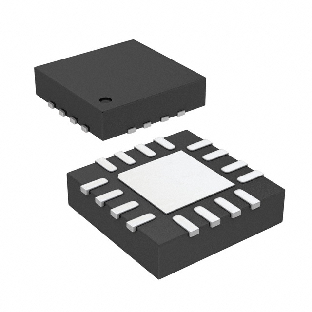
- Part No.:
- LTC6820HUD#PBF
- Manufacturer:
- Analog Devices Inc.
- Category:
- Specialized
- Package:
- 16-WFQFN Exposed Pad
- Datasheet:
-
 LTC6820HUD#PBF.pdf
- Description:
- IC INTERFACE SPECIALIZED 16QFN
- Quantity:
- Payment:

- Shipping:

Inventory:1,580
Please send an inquiry. Send us your inquiry, and we will respond immediately.
Product details
Overview
LTC6820HUD#PBF from Analog Devices is an isoSPI isolated bidirectional communications interface IC that enables SPI signal transmission across galvanic isolation barriers via a single twisted-pair cable. It operates from 2.7V to 5.5V, supports 1Mbps data rate over up to 100m CAT-5 cable, and features ultralow 2µA idle current, automatic wake-up detection, and AEC-Q100 qualification for automotive battery monitoring systems.
For engineers reviewing the LTC6820HUD#PBF datasheet, LTC6820HUD#PBF pinout, LTC6820HUD#PBF application, or LTC6820HUD#PBF equivalent, this page delivers verified technical context, exact pin functions, real-world timing behavior under SLOW/MSTR configuration, and validated alternatives for isolated SPI system design in harsh EMI environments.
Technical Context
The LTC6820HUD#PBF implements a transformer-coupled isoSPI physical layer using matched source/sink current drivers on IP/IM pins, eliminating center-tap requirements and reducing EMI. Its receiver employs precision window comparators with threshold set by ICMP voltage (0.2–1.5V), enabling configurable noise immunity via external resistor divider on IBIAS.
It supports two operational modes: master (MSTR = VDD) for microcontroller-side interface and slave (MSTR = GND) for remote sensor or battery monitor side. Timing is configurable via SLOW pin - low for >200kHz operation (e.g., 1MHz at tCLK = 0.5µs), high for robustness at lower frequencies with extended pulse widths.
Key Specifications
| Parameter | Value and Actual Design Meaning |
|---|---|
| Data Rate | 1Mbps maximum; enables real-time cell voltage polling in 96-cell BMS stacks with sub-10µs per-byte latency. |
| Cable Length | Up to 100 meters over twisted pair; supports distributed battery packs in EV traction systems without repeaters. |
| Idle Current | 1µA (MSTR = VDD) or 2µA (MSTR = GND); extends sleep-mode runtime in always-on automotive monitoring nodes. |
| Wake-Up Latency | 8µs max from CS fall or IP/IM edge detection; ensures responsive command execution after deep sleep. |
| Supply Range | VDD = 2.7–5.5V; VDDS = 1.7–5.5V; allows independent level-shifting of SPI I/O to match host MCU logic (e.g., 1.8V/3.3V/5V). |
| Operating Temp | –40°C to +125°C (H-grade); qualified per AEC-Q100 Grade 0; suitable for under-hood battery disconnect units. |
| Isolation Robustness | Compatible with standard 1:1 pulse transformers; achieves >500Vrms working isolation with proper layout and termination. |
Pinout & Package
Package: 16-lead (3mm × 3mm) plastic QFN (UD package), exposed pad (Pin 17) optional GND connection, MSL 1, –40°C to +125°C operating range.
| Pin/Terminal | Circuit Role | Design Meaning |
|---|---|---|
| MOSI (Pin 1) | SPI Master Out / Slave In Data | Open-drain output (slave) or input (master); requires external pull-up to VDDS; carries serialized command data from MCU or to slave device. |
| MISO (Pin 2) | SPI Master In / Slave Out Data | Open-drain output (master) or input (slave); returns readback data (e.g., cell voltages) across isolation barrier. |
| SCK (Pin 3) | SPI Clock Input/Output | Push-pull output (slave) or input (master); clock edge timing defines MOSI/MISO sampling; polarity/phase configurable via POL/PHA pins. |
| CS (Pin 4) | SPI Chip Select Input/Output | Push-pull output (slave) or input (master); long ±1 pulses encode CS transitions; triggers wake-up and frame synchronization. |
| VDDS (Pin 5) | SPI I/O Power Supply | Sets logic thresholds for CS/SCK/MOSI/MISO/EN; enables level shifting between host MCU and isolated domain. |
| POL (Pin 6) | SPI Clock Polarity Control | Tied to VDD/GND to select SCK idle state (low = Mode 0/1, high = Mode 2/3); determines latch edge relative to clock phase. |
| PHA (Pin 7) | SPI Clock Phase Control | Tied to VDD/GND to select data sampling edge (0 = first edge, 1 = second edge); supports all four standard SPI modes. |
| VDD (Pin 8) | Main Device Power Supply | Bypassed with ≥0.01µF capacitor; powers internal bias circuits, drivers, and logic; independent from VDDS for flexible supply partitioning. |
| IM (Pin 9) | Isolated Interface Minus | Differential transmitter/receiver terminal; paired with IP to drive/receive isoSPI pulses; connects to transformer secondary winding. |
| IP (Pin 10) | Isolated Interface Plus | Differential transmitter/receiver terminal; complements IM; differential amplitude VA = |VIP – VIM| set by IBIAS current and RM termination. |
| MSTR (Pin 11) | Master/Slave Configuration | Hardwired to VDD (master) or GND (slave); configures directionality, wake-up source (CS vs IP/IM), and return pulse generation logic. |
| SLOW (Pin 12) | Timing Mode Selection | Low = fast mode (t½PW = 40–60ns); high = slow mode (t½PW = 0.9–1.4µs); used to meet timing margins with long cables or marginal transformers. |
| GND (Pin 13) | Device Ground Reference | Analog/digital ground common point; must be low-impedance; exposed pad (Pin 17) may connect here to improve thermal performance. |
| ICMP (Pin 14) | Comparator Threshold Set | Connected to resistor divider from IBIAS; sets receiver threshold VTCMP = 0.5 × VICMP; adjusts noise immunity vs sensitivity trade-off. |
| IBIAS (Pin 15) | Interface Bias Current Source | Sinks current IB = 2V/RBIAS; sets IP/IM drive current IDRV = 20 × IB; RBIAS = 2kΩ–20kΩ (1% tolerance) for 0.1–1mA range. |
| EN (Pin 16) | Enable Override Input | Active-high; forces READY state regardless of CS/IP/IM activity; disables auto-idle timeout; used for forced wake-up or debug hold. |
Key Features
| Feature | Design Value |
|---|---|
| Transformer-based galvanic isolation | Eliminates need for center-tapped transformers or capacitive isolators; reduces BOM cost and EMI emissions in high-voltage battery systems. |
| Configurable noise immunity | Receiver threshold (VTCMP) and drive amplitude (VA) independently adjusted via IBIAS/ICMP resistors to optimize SNR for specific cable length and environment. |
| Automatic wake-up with 8µs latency | Enables ultra-low-power monitoring: device sleeps at 1–2µA, wakes instantly on CS transition or isoSPI pulse, resumes full SPI operation within one clock cycle. |
| AEC-Q100 Grade 0 qualification | Validated for automotive under-hood use (–40°C to +125°C); includes HTOL, temperature cycling, and ESD testing per ISO 16750 and AEC standards. |
| No software changes required | Transparently bridges standard SPI protocol; no driver modification needed on MCU or slave side; compatible with existing SPI stack and HAL layers. |
Applications
| Battery Management Systems | Industrial Sensor Networks |
|---|---|
|
Use Scenario: Monitoring 12–96 series-connected Li-ion cells in electric vehicle traction batteries, with isolation between high-voltage stack and 12V MCU domain. IC Role / Device Role / Timing Role: LTC6820HUD#PBF acts as isolated SPI bridge, converting MCU SPI commands into isoSPI pulses sent across transformer-isolated twisted pair to LTC681x monitor ICs. Use Value: Enables safe, high-speed cell voltage acquisition (≤10ms for full stack) while meeting reinforced isolation requirements (>500Vrms) and AEC-Q100 reliability. |
Use Scenario: Connecting distributed pressure/temperature sensors in oil & gas pipeline monitoring, located up to 100m from central controller in explosive environments. IC Role / Device Role / Timing Role: LTC6820HUD#PBF serves as isolated slave interface, receiving SPI commands from central PLC and returning sensor readings over intrinsically safe twisted-pair wiring. Use Value: Provides certified galvanic isolation without optocouplers or custom ASICs; supports 1Mbps data rate for sub-second sensor update cycles in Class I Div 2 zones. |
| Automotive ADAS Domain Controllers | Renewable Energy Storage Systems |
|
Use Scenario: Isolating radar/EPS control signals between ASIL-D domain controller and peripheral actuators in autonomous driving platforms. IC Role / Device Role / Timing Role: LTC6820HUD#PBF operates in master mode on domain controller side, transmitting safety-critical SPI commands across isolation barrier to slave-side motor drivers. Use Value: Meets ISO 26262 functional safety requirements for communication channel; built-in wake-up and low idle current reduce power consumption in always-on ADAS modules. |
Use Scenario: Interfacing battery string monitors in grid-scale lithium iron phosphate (LFP) energy storage systems, where DC bus voltages exceed 1000V. IC Role / Device Role / Timing Role: LTC6820HUD#PBF functions as slave-side interface, translating isoSPI pulses from central BMS controller into local SPI signals for multi-cell monitor ICs. Use Value: Supports 100m inter-rack cabling without repeaters; configurable drive strength and threshold ensure reliable operation despite long-cable attenuation and switching noise from inverters. |
Equivalent & Alternatives
The following parts are listed as comparable options for similar isolated SPI interface applications.
| Alternative Part | Technical Difference | Application Difference | Selection Advice |
|---|---|---|---|
| ADuM3401CRWZ | Quad-channel digital isolator (non-SPI-specific); uses iCoupler® capacitive isolation; requires external SPI controller logic; no integrated isoSPI encoding/decoding. | Needs discrete level shifters and SPI state machine; higher component count; not optimized for transformer-based long-cable SPI extension. | Select when needing general-purpose isolation channels or mixed-signal isolation; avoid when direct isoSPI compatibility and transformer simplicity are required. |
| SI8641ED-B-IS | Quad-channel digital isolator with integrated refresh logic; 150Mbps max data rate; 5kVrms isolation; no native isoSPI protocol handling or cable-length optimization. | Requires external SPI-to-isolated-logic translation; lacks automatic wake-up, configurable thresholds, or cable-length-aware timing modes. | Prefer for high-speed digital isolation in short-reach applications (<1m); not suitable for 100m twisted-pair isoSPI deployment or automotive BMS. |
Compared with ADuM3401CRWZ and SI8641ED-B-IS, the LTC6820HUD#PBF delivers turnkey isoSPI functionality - including pulse encoding, wake-up detection, cable-length-adaptive timing, and transformer-optimized drive - in a single chip, reducing system complexity and validation effort for automotive and industrial battery monitoring.
Availability
LTC6820HUD#PBF is available at Aetrix Electronics and suitable for battery management systems, automotive ADAS domain controllers, and industrial sensor networks requiring stable component supply, AEC-Q100 compliance, and long-cable isolated SPI connectivity.
Supply support for LTC6820HUD#PBF includes scheduled delivery planning, volume procurement assistance, BOM continuity management, traceable sourcing, and lifecycle availability coordination for OEM customers, industrial embedded developers, connected-device designers, and electronics production programs.
Manufacturer
Analog Devices is a global leader in high-performance analog, mixed-signal, and digital signal processing semiconductors, serving industrial, automotive, communications, and healthcare markets.
The LTC6820HUD#PBF belongs to Analog Devices' isoSPI product line, engineered specifically to replace optocouplers and discrete isolator solutions in high-reliability battery monitoring and distributed sensing applications demanding robust galvanic isolation over extended distances.
FAQ
What is the maximum supported cable length for LTC6820HUD#PBF in a real-world automotive BMS installation?
The LTC6820HUD#PBF supports up to 100 meters of CAT-5 twisted-pair cable at 1Mbps, as verified in Analog Devices' reference designs and AEC-Q100 test reports. In production EV battery packs, typical deployments achieve 60–80m with 120Ω termination and 1:1 pulse transformers, maintaining <10⁻¹² BER under ISO 11452-4 burst noise. Cable length is limited by pulse distortion-not data rate-so derating applies beyond 80m in high-EMI engine bays.
Does LTC6820HUD#PBF require external components to operate, and which ones are mandatory?
Yes, LTC6820HUD#PBF requires three mandatory external components: (1) a resistor divider (RBIAS = RB1 + RB2, 2kΩ–20kΩ) between IBIAS and GND to set drive current and comparator threshold; (2) a 100Ω termination resistor (RM) across IP/IM at each end of the twisted pair; and (3) ≥0.01µF bypass capacitors on VDD and VDDS. Optional components include pull-ups on MOSI/MISO and transformer selection per isolation voltage rating.
How does LTC6820HUD#PBF handle simultaneous communication from multiple slave devices on the same twisted pair?
The LTC6820HUD#PBF supports multidrop configurations only in slave mode (MSTR = GND), where slaves transmit only short –1 pulses (when MISO = 0) and never long or +1 pulses. This prevents bus collisions because only the master initiates CS transitions and data latching. Multiple slaves share the same IP/IM pair but respond individually based on decoded CS address framing - confirmed in LTC6820 datasheet Section "Multidrop" and Figure 11.
Can LTC6820HUD#PBF interface directly with 1.8V microcontrollers without level-shifting circuitry?
Yes, LTC6820HUD#PBF supports 1.7V to 5.5V VDDS, allowing direct connection to 1.8V MCUs. When VDDS = 1.8V, VIH(SPI) = 0.8 × 1.8V = 1.44V min and VOL = 0.2V max, matching standard 1.8V logic thresholds. No external level shifters are needed - the LTC6820HUD#PBF's VDDS pin powers its SPI I/O buffers and defines their voltage thresholds natively.
What is the role of the SLOW pin on LTC6820HUD#PBF, and when should it be asserted high?
The SLOW pin selects isoSPI timing mode: low enables fast mode (t½PW = 40–60ns) for ≤1MHz operation; high enables slow mode (t½PW = 0.9–1.4µs) for robustness with long cables (>50m), marginal transformers, or noisy environments. Assert SLOW = high when measured tRISE on IP/IM exceeds 110ns (per datasheet Note 8), or when timing violations occur during startup with MSTR = 0 slave devices.
LTC6820HUD#PBF Specifications
- Product attributes
- Attribute value
- Manufacturer:
- Analog Devices Inc.
- Series:
- isoSPI
- Package/Case:
- 16-WFQFN Exposed Pad
- Packaging:
- Tube
- Product Status:
- Active
- Applications:
- Isolated Communications Interface
- Interface:
- SPI
- Voltage - Supply:
- 2.7V ~ 5.5V
- Supplier Device Package:
- 16-QFN (3x3)
- Grade:
- -
- Qualification:
- -
- Mounting Type:
- Surface Mount
LTC6820HUD#PBF FAQ
1.How can I place an order for LTC6820HUD#PBF through Aetrix?
Please submit a Request for Quotation (RFQ) for LTC6820HUD#PBF on Aetrix. Our sales agent will provide a competitive quotation and guide you through the order confirmation once you accept the terms.
2.Are the price and stock information for LTC6820HUD#PBF reliable?
The price and inventory of LTC6820HUD#PBF are updated periodically and may fluctuate due to market conditions. Stock and pricing data are typically refreshed every 24 hours. Quotation validity for LTC6820HUD#PBF is usually 5 days.
3.What payment methods are accepted for LTC6820HUD#PBF?
We accept Wire Transfer, PayPal, Credit Card, Western Union, MoneyGram, and Escrow for LTC6820HUD#PBF transactions.
Note: Certain payment methods may incur a processing fee.
4.How is shipping managed for LTC6820HUD#PBF?
LTC6820HUD#PBF orders can be shipped via leading logistics carriers, including DHL, UPS, FedEx, TNT, or Registered Mail.
Once your LTC6820HUD#PBF order is processed, you will receive an email with the shipment details and tracking number.
Note: Tracking information may take up to 24 hours to appear. Express delivery typically takes 3–5 business days.
5.How can I obtain technical support or documentation for LTC6820HUD#PBF?
For technical support, including LTC6820HUD#PBF datasheets, pinout diagrams, or application guidance, please contact our engineering support team. They can provide detailed documentation and assistance for your LTC6820HUD#PBF requirements.
6.How does Aetrix verify that LTC6820HUD#PBF is sourced from the original manufacturer or authorized distributors?
All LTC6820HUD#PBF products on Aetrix are procured from qualified distributors and authorized channels. Our dedicated quality assurance team conducts strict verification, including traceability checks and, if necessary, third-party testing. This ensures that LTC6820HUD#PBF meets industry standards.
7.What is the process for return or replacement of LTC6820HUD#PBF?
All LTC6820HUD#PBF units undergo pre-shipment inspection (PSI). If there is an issue with LTC6820HUD#PBF, returns or replacements are accepted under the following conditions:
1.Quantity discrepancies, incorrect items, or visible external defects (such as breakage or corrosion), acknowledged by Aetrix.
2.The issue is reported within 90 days of delivery.
3.The LTC6820HUD#PBF part is unused and in its original packaging.
Return procedure for LTC6820HUD#PBF:
1.Submit a request within 90 days.
2.Obtain a Return Material Authorization (RMA) from Aetrix.
LTC6820HUD#PBF Tags

-
NVT4857UKAZ
NXP Semiconductors

-
TCA8418RTWR
Texas Instruments

-
PCA9546APWR
Texas Instruments

-
MD0100N8-G
Microchip Technology

-
PCA9548APW,118
NXP Semiconductors

-
PCA9540BDP,118
NXP Semiconductors

-
PCA9548APWR
Texas Instruments

-
PCA9546APW,118
NXP Semiconductors

-
PTN3360DBS,518
NXP Semiconductors

-
PCA9546ABS,118
NXP Semiconductors

-
PCA9518PWR
Texas Instruments

-
PCA9545APW,118
NXP Semiconductors
Tech Hub

A practical engineering guide to 3.3V and 5V logic compatibility, input thresholds, resistor dividers, translator ICs, MOSFET level shifting, I2C pull-ups, timing limits and power-sequencing risks.

The 74HC595 uses push-pull logic outputs, while the TPIC6B595 uses 50 V open-drain DMOS sinks for higher-power loads. This guide compares timing, current limits, 3.3 V interfacing, load wiring, thermal…

The 74HC595 converts serial data into eight stable parallel outputs. This guide covers pin functions, shift and storage timing, OE and MR behavior, drive-current limits, cascading, voltage compatibilit…

A technical comparison of level-sensitive latches and edge-triggered flip-flops, covering timing windows, setup and hold limits, master–slave operation, time borrowing, race-through, HDL inference and…

A D latch stores one bit while Enable controls when data can pass. This reference covers gate-level operation, truth tables, transparency, setup and hold timing, LE versus OE, common ICs and practical …

An SR latch stores one bit through cross-coupled feedback. This engineering reference covers NOR and NAND implementations, truth tables, forbidden-state recovery, gated operation, switch debouncing, fa…

Latch circuits retain one bit through feedback. This technical reference covers SR and D latches, truth tables, transparency, timing limits, latch-versus-flip-flop behavior, applications and common log…

An engineering guide to LED driver operation, constant-current and constant-voltage outputs, linear and switching topologies, dimming, IC selection, calculations, replacement compatibility, and fault c…

Operational amplifier guide covering op amp basics, feedback, ideal vs real op amps, common configurations, buffer circuits, offset, bias current, gain-bandwidth, slew rate, rail-to-rail limits and sel…

Jumper cables guide covering safe connection order, red and black clamp placement, final ground connection, cable gauge, length, clamp quality, copper vs CCA cables, jump starter comparison and battery…


