
 My Inquiry
 My Account


Renesas M306N5FCTFP#B0J
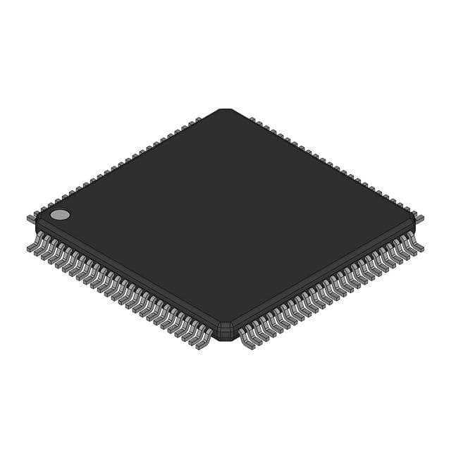
- Part No.:
- M306N5FCTFP#B0J
- Manufacturer:
- Renesas
- Category:
- Microcontrollers
- Package:
- 100-BQFP
- Datasheet:
-
 M306N5FCTFP#B0J.pdf
- Description:
- 16-BIT, FLASH, M16C CPU
- Quantity:
- Payment:

- Shipping:

Inventory:260
Please send an inquiry. Send us your inquiry, and we will respond immediately.
Product details
Overview
CYRF6936 from Cypress Semiconductor is a 2.4 GHz WirelessUSB™ LP Radio SoC integrating DSSS/GFSK transceiver, 16-byte TX/RX FIFOs, Auto Transaction Sequencer (ATS), Power Management Unit (PMU), and SPI interface - delivering up to +4 dBm output power, –97 dBm receive sensitivity, and 1 Mbps GFSK data rate for ultra-low-power wireless peripherals.
For engineers reviewing the CYRF6936 datasheet, CYRF6936 pinout, CYRF6936 application, or CYRF6936 equivalent, this page provides verified technical context, validated pin functions, real-world use cases in battery-operated human-interface devices, and confirmed alternative parts with documented functional trade-offs.
Technical Context
The CYRF6936 implements a dual-conversion low-IF 2.4 GHz radio architecture with integrated PA, LNA, and RSSI circuitry, supporting 98 discrete 1 MHz ISM channels and fast synthesizer settling (≤100 µs on 25 designated "fast" channels). Its baseband handles DSSS spreading/despreading, SOP/EOP detection, CRC16 generation/checking, and AutoRate™ dynamic data rate adaptation.
It features an autonomous Auto Transaction Sequencer (ATS) that executes full transmit–ACK or receive–ACK sequences without MCU intervention for ≤16-byte packets, while its PMU delivers regulated 1.8 V logic supply and configurable 2.4–2.7 V VREG output (up to 15 mA) directly from 1.8–3.6 V battery input - enabling coin-cell operation without external regulators.
Key Specifications
| Parameter | Value and Actual Design Meaning |
|---|---|
| Operating Frequency | 2.400–2.483 GHz ISM band - globally license-free operation compliant with FCC Part 15, ETSI EN 300 328, and ARIB T-66. |
| Transmit Output Power | +4 dBm maximum (7-step programmable down to –35 dBm) - enables flexible range/power tuning and coexistence in dense RF environments. |
| Receive Sensitivity | –97 dBm at 250 kbps DSSS - supports reliable link budget up to ~30 m line-of-sight in typical indoor conditions. |
| Data Rates | 1 Mbps (GFSK), 250/125 kbps (8DR), 62.5/31.25/15.625 kbps (DDR/SDR) - selectable per-link for adaptive interference resilience. |
| Sleep Current | <1 µA - allows multi-year operation on CR2032 coin cell when paired with ATS-driven burst transmission. |
| Supply Voltage Range | 1.8 V to 3.6 V - direct compatibility with single-cell Li-ion, Li-poly, or alkaline/coin-cell sources without external LDO. |
| SPI Interface | 4 MHz max clock, 3- or 4-pin mode, register-accessible while in sleep - enables low-latency configuration and firmware-less wake-up control. |
Pinout & Package
40-pin QFN package (6 × 6 mm, 0.5 mm pitch) with exposed thermal pad (E-PAD) requiring solder connection to ground plane for thermal and electrical integrity.
| Pin/Terminal | Circuit Role | Design Meaning |
|---|---|---|
| VBAT0/1/2 | Main power supply inputs | Accept 1.8–3.6 V battery input; decoupled individually to minimize noise coupling between analog/radio/logic domains. |
| VCC | Internal regulator output supply | 2.4–3.6 V supply for internal digital logic; typically tied to VREG or external LDO output. |
| RFP / RFN | Differential RF antenna interface | 50 Ω matched differential port; requires balun or matching network for single-ended antenna connection. |
| XTAL | Crystal oscillator input | Direct 12 MHz fundamental-mode crystal connection (no load caps required); ±30 ppm stability mandated. |
| SS / SCK / MOSI / MISO | SPI bus interface | Full-duplex 4-pin or 3-pin (SDAT) SPI; operates during sleep for register access and wake-up triggering. |
| IRQ | Configurable interrupt output | Active-HIGH/LOW, CMOS/open-drain; signals packet RX/TX completion, RSSI threshold, or low-battery event. |
| PACTL | External PA/T/R switch control | GPIO-configurable output to drive external power amplifier or antenna switch - synchronized with RF activity. |
| XOUT | Programmable clock output | 0.75/1.5/3/6/12 MHz buffered clock; usable to drive external MCU or sensor timing without additional oscillator. |
Key Features
| Feature | Design Value |
|---|---|
| Auto Transaction Sequencer (ATS) | Executes complete TX–ACK or RX–ACK handshakes autonomously - eliminates MCU polling and reduces firmware overhead for HID-class devices. |
| Power Management Unit (PMU) | Generates regulated 1.8 V logic rail and configurable 2.4–2.7 V VREG (15 mA max) from raw battery - removes need for external boost converters in coin-cell designs. |
| Dynamic Data Rate (AutoRate™) | Automatically selects optimal data rate (15.6–1000 kbps) based on RSSI and link quality - maintains robustness across varying distance/interference without host intervention. |
| Low-Noise Amplifier (LNA) Control | Manual LNA gain adjustment (±20 dB) and 30 dB attenuation enable precise receiver dynamic range tuning - critical for short-range high-SNR applications like gamepad-to-PC links. |
| Separate 16-byte TX/RX FIFOs | Enables burst SPI loading of full packet before transmission and interrupt-driven retrieval after reception - simplifies timing-critical MCU integration. |
Applications
| Wireless Keyboards | Wireless Gamepads |
|---|---|
|
Use Scenario: Battery-powered keyboard transmitting keystroke events to PC or tablet via 2.4 GHz link with <100 ms latency and multi-year runtime. IC Role / Device Role / Timing Role: Full-featured Radio SoC handling RF modulation, packet framing, ACK management, and power-gated sleep/wake cycles. Use Value: ATS-driven transaction mode ensures zero-latency keypress response without MCU polling; sub-1 µA sleep current extends CR2032 life beyond 36 months. |
Use Scenario: Low-latency controller for gaming consoles requiring jitter-free button/axis reporting and rapid channel-hopping to avoid Wi-Fi interference. IC Role / Device Role / Timing Role: Integrated transceiver with fast synthesizer settling (≤100 µs) and AutoRate™ adapts data rate dynamically to maintain link integrity during motion-induced signal fade. Use Value: 1 Mbps GFSK mode delivers <2 ms round-trip latency; programmable PA output (+4 dBm) ensures reliable 10+ meter range even behind metal enclosures. |
| Remote Controls | Home Automation Sensors |
|
Use Scenario: IR-replacement remote using push-button wake-up and short-burst transmission of command packets to set-top box or smart TV. IC Role / Device Role / Timing Role: Ultra-low-power SoC with hardware-accelerated packet framing, CRC16, and auto-ACK - enabling single-button press to full RF transmission in <15 ms. Use Value: Sleep current <1 µA and fast crystal startup allow immediate transmission upon button press; RSSI monitoring enables proximity-based UI feedback. |
Use Scenario: Battery-powered temperature/humidity sensor node in smart home system transmitting periodic readings every 30 seconds to gateway. IC Role / Device Role / Timing Role: Self-contained wireless modem with integrated PMU supplying regulated voltage to external sensor ICs and managing battery voltage monitoring. Use Value: Configurable low-battery IRQ alerts user before failure; VREG output powers sensor and MCU simultaneously - reducing BOM count by one regulator. |
Equivalent & Alternatives
The following parts are listed as comparable options for similar 2.4 GHz ISM-band radio SoC applications.
| Alternative Part | Technical Difference | Application Difference | Selection Advice |
|---|---|---|---|
| Nordic nRF24L01+ | Lacks integrated PMU and ATS; requires external regulator and MCU-managed ACK sequencing; 2 Mbps GFSK but lower sensitivity (–80 dBm). | Better suited for higher-throughput, MCU-rich systems where host handles protocol stack; less optimal for ultra-low-power HID with minimal firmware. | Select when needing >1 Mbps throughput and existing MCU resources to manage link layer; avoid when minimizing firmware complexity or battery size is critical. |
| Silicon Labs Si4463 | Sub-GHz only (434/868/915 MHz); no 2.4 GHz support; higher sensitivity (–126 dBm) but incompatible frequency band. | Designed for long-range, low-data-rate IoT sensors (e.g., utility meters); cannot replace CYRF6936 in 2.4 GHz consumer HID applications. | Choose only for sub-GHz regulatory compliance or extreme range requirements; not a functional substitute for CYRF6936's 2.4 GHz WirelessUSB™ LP ecosystem. |
Compared with Nordic nRF24L01+ and Silicon Labs Si4463, the CYRF6936 uniquely combines 2.4 GHz ISM operation, hardware ATS, integrated PMU, and sub-1 µA sleep - making it the only option among the three qualified for coin-cell-powered, firmware-light wireless keyboards and gamepads requiring certified interoperability with legacy WirelessUSB™ hosts.
Availability
CYRF6936 is available at Aetrix Electronics and suitable for wireless human-interface devices, battery-constrained remote controls, and low-latency gaming peripherals requiring stable component supply, long-term lifecycle assurance, and full regulatory documentation support.
Supply support for CYRF6936 includes scheduled delivery planning, volume procurement assistance, BOM continuity management, traceable sourcing, and lifecycle availability coordination for OEM customers, industrial embedded developers, connected-device designers, and electronics production programs.
Manufacturer
Cypress Semiconductor (now part of Infineon Technologies) is a fabless semiconductor company specializing in programmable system-on-chip (PSoC), memory, and connectivity solutions for industrial, automotive, and consumer markets.
The CYRF6936 belongs to Cypress's WirelessUSB™ LP Radio SoC product line, engineered specifically for ultra-low-power, cost-sensitive 2.4 GHz human-interface devices requiring seamless interoperability with existing USB wireless dongles and minimal host-side driver changes.
FAQ
What is the primary function of the CYRF6936 in a wireless system?
The CYRF6936 serves as a complete 2.4 GHz WirelessUSB™ LP Radio SoC, integrating transceiver, packet framer, Auto Transaction Sequencer (ATS), Power Management Unit (PMU), and SPI interface. It enables self-contained wireless communication for HID devices without requiring external regulators or complex MCU firmware - the CYRF6936 handles modulation, ACK generation, sleep/wake timing, and battery regulation internally.
Does the CYRF6936 support direct connection to a coin-cell battery?
Yes, the CYRF6936 supports direct connection to a single CR2032 coin cell (nominal 3 V) via its VBAT pins. Its integrated PMU regulates down to 1.8 V logic supply and provides configurable VREG output, while its <1 µA sleep current enables multi-year operation - confirmed in Cypress Application Note AN72202 for CYRF6936-based keyboard reference designs.
Can the CYRF6936 interoperate with first-generation WirelessUSB™ devices?
Yes, the CYRF6936 is explicitly designed for interoperability with first-generation CYWUSB69xx devices, as stated in the Functional Description section of datasheet 38-16015 Rev. *K. This backward compatibility ensures seamless integration into existing WirelessUSB™ ecosystems, including certified USB dongles and host drivers, without firmware or protocol modifications.
What is the role of the Auto Transaction Sequencer (ATS) in the CYRF6936?
The ATS automates full packet transactions: for transmission, it starts the crystal/synthesizer, sends the payload, switches to receive mode, and waits for ACK - all without MCU intervention. For reception, it automatically replies with ACK upon valid packet detection. This feature is fully operational for ≤16-byte packets and is central to the CYRF6936's low-firmware-footprint design philosophy.
Is an external crystal required for CYRF6936 operation, and what are its specifications?
Yes, a 12 MHz fundamental-mode parallel-resonant crystal with ±30 ppm stability, <60 Ω series resistance, 10 pF load capacitance, and ≤100 µW drive level must be connected directly between XTAL and GND - no external capacitors needed. This specification is mandatory for guaranteed timing accuracy, synthesizer lock, and regulatory compliance per datasheet Section "Clocks".
M306N5FCTFP#B0J Specifications
- Product attributes
- Attribute value
- Manufacturer:
- Renesas
- Package/Case:
- 100-BQFP
- Series:
- M16C™ M16C/60/6N5
- Packaging:
- Bulk
- Product Status:
- Active
- Programmable:
- Not Verified
- Core Processor:
- M16C/60
- Core Size:
- 16-Bit
- Speed:
- 20MHz
- Connectivity:
- CANbus, I2C, IEBus, SIO, UART/USART
- Peripherals:
- DMA, WDT
- Number of I/O:
- 87
- Program Memory Size:
- 128KB (128K x 8)
- Program Memory Type:
- FLASH
- EEPROM Size:
- 4K x 8
- RAM Size:
- 5K x 8
- Voltage - Supply (Vcc/Vdd):
- 4.2V ~ 5.5V
- Data Converters:
- A/D 26x10b; D/A 2x8b
- Oscillator Type:
- Internal
- Operating Temperature:
- -40°C ~ 85°C (TA)
- Grade:
- -
- Qualification:
- -
- Mounting Type:
- Surface Mount
- Supplier Device Package:
M306N5FCTFP#B0J FAQ
1.How can I place an order for M306N5FCTFP#B0J through Aetrix?
Please submit a Request for Quotation (RFQ) for M306N5FCTFP#B0J on Aetrix. Our sales agent will provide a competitive quotation and guide you through the order confirmation once you accept the terms.
2.Are the price and stock information for M306N5FCTFP#B0J reliable?
The price and inventory of M306N5FCTFP#B0J are updated periodically and may fluctuate due to market conditions. Stock and pricing data are typically refreshed every 24 hours. Quotation validity for M306N5FCTFP#B0J is usually 5 days.
3.What payment methods are accepted for M306N5FCTFP#B0J?
We accept Wire Transfer, PayPal, Credit Card, Western Union, MoneyGram, and Escrow for M306N5FCTFP#B0J transactions.
Note: Certain payment methods may incur a processing fee.
4.How is shipping managed for M306N5FCTFP#B0J?
M306N5FCTFP#B0J orders can be shipped via leading logistics carriers, including DHL, UPS, FedEx, TNT, or Registered Mail.
Once your M306N5FCTFP#B0J order is processed, you will receive an email with the shipment details and tracking number.
Note: Tracking information may take up to 24 hours to appear. Express delivery typically takes 3–5 business days.
5.How can I obtain technical support or documentation for M306N5FCTFP#B0J?
For technical support, including M306N5FCTFP#B0J datasheets, pinout diagrams, or application guidance, please contact our engineering support team. They can provide detailed documentation and assistance for your M306N5FCTFP#B0J requirements.
6.How does Aetrix verify that M306N5FCTFP#B0J is sourced from the original manufacturer or authorized distributors?
All M306N5FCTFP#B0J products on Aetrix are procured from qualified distributors and authorized channels. Our dedicated quality assurance team conducts strict verification, including traceability checks and, if necessary, third-party testing. This ensures that M306N5FCTFP#B0J meets industry standards.
7.What is the process for return or replacement of M306N5FCTFP#B0J?
All M306N5FCTFP#B0J units undergo pre-shipment inspection (PSI). If there is an issue with M306N5FCTFP#B0J, returns or replacements are accepted under the following conditions:
1.Quantity discrepancies, incorrect items, or visible external defects (such as breakage or corrosion), acknowledged by Aetrix.
2.The issue is reported within 90 days of delivery.
3.The M306N5FCTFP#B0J part is unused and in its original packaging.
Return procedure for M306N5FCTFP#B0J:
1.Submit a request within 90 days.
2.Obtain a Return Material Authorization (RMA) from Aetrix.
M306N5FCTFP#B0J Tags

-
ATTINY4-TSHR
Microchip Technology
-
ATTINY10-TSHR
Microchip Technology
-
ATTINY10-TS8R
Microchip Technology

-
ATTINY202-SSNR
Microchip Technology
-
ATTINY202-SSFR
Microchip Technology
-
ATTINY402-SSNR
Microchip Technology

-
PIC16F15213T-I/MF
Microchip Technology
-
PIC16F15213-E/MF
Microchip Technology

-
PIC10F200T-I/OT
Microchip Technology
-
ATTINY412-SSNR
Microchip Technology
-
PIC10F202T-I/OT
Microchip Technology

-
ATTINY404-SSNR
Microchip Technology
Tech Hub

TTL and CMOS logic families differ in thresholds, loading, output drive, power and timing. This engineering guide compares 74HC and 74HCT, calculates noise margins and checks 3.3 V/5 V compatibility.

A practical engineering guide to 3.3V and 5V logic compatibility, input thresholds, resistor dividers, translator ICs, MOSFET level shifting, I2C pull-ups, timing limits and power-sequencing risks.

The 74HC595 uses push-pull logic outputs, while the TPIC6B595 uses 50 V open-drain DMOS sinks for higher-power loads. This guide compares timing, current limits, 3.3 V interfacing, load wiring, thermal…

The 74HC595 converts serial data into eight stable parallel outputs. This guide covers pin functions, shift and storage timing, OE and MR behavior, drive-current limits, cascading, voltage compatibilit…

A technical comparison of level-sensitive latches and edge-triggered flip-flops, covering timing windows, setup and hold limits, master–slave operation, time borrowing, race-through, HDL inference and…

A D latch stores one bit while Enable controls when data can pass. This reference covers gate-level operation, truth tables, transparency, setup and hold timing, LE versus OE, common ICs and practical …

An SR latch stores one bit through cross-coupled feedback. This engineering reference covers NOR and NAND implementations, truth tables, forbidden-state recovery, gated operation, switch debouncing, fa…

Latch circuits retain one bit through feedback. This technical reference covers SR and D latches, truth tables, transparency, timing limits, latch-versus-flip-flop behavior, applications and common log…

An engineering guide to LED driver operation, constant-current and constant-voltage outputs, linear and switching topologies, dimming, IC selection, calculations, replacement compatibility, and fault c…

Operational amplifier guide covering op amp basics, feedback, ideal vs real op amps, common configurations, buffer circuits, offset, bias current, gain-bandwidth, slew rate, rail-to-rail limits and sel…


