
 My Inquiry
 My Account


STMicroelectronics M41ST87WMX6TR
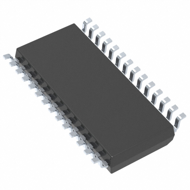
- Part No.:
- M41ST87WMX6TR
- Manufacturer:
- STMicroelectronics
- Category:
- Real Time Clocks
- Package:
- 28-SOIC (0.295", 7.50mm Width)
- Datasheet:
-
 M41ST87WMX6TR.pdf
- Description:
- IC RTC CLOCK/CALENDAR I2C 28SO
- Quantity:
- Payment:

- Shipping:

Inventory:4,044
Please send an inquiry. Send us your inquiry, and we will respond immediately.
Product details
Overview
M41ST87WMX6TR from STMicroelectronics is a secure serial real-time clock (RTC) and non-volatile RAM (NVRAM) supervisor IC with integrated 32.768 kHz crystal, tamper detection, 128 bytes of clearable user NVRAM, I²C interface (400 kHz), and dual power-fail comparators. It operates at 3.0–3.6 V, provides battery-backed timekeeping down to 500 nA typical supply current, and delivers microprocessor power-on reset and programmable alarm/interrupt functions. Used in industrial security systems requiring time-stamped tamper response and secure data retention during main power loss.
For engineers reviewing the M41ST87WMX6TR datasheet, M41ST87WMX6TR pinout, M41ST87WMX6TR application, or M41ST87WMX6TR equivalent, this page details its RTC/calendar register map (BCD format), tamper timestamping logic, VPFD thresholds (2.63 V / 2.9 V), embedded crystal isolation, and SOX28 package-specific features including TPCLR and EX pins.
Technical Context
The M41ST87WMX6TR integrates a crystal-controlled RTC core with binary-coded decimal (BCD) time registers covering tenths/hundredths of seconds through century, automatic leap-year correction, and full-time 32 kHz square wave output (F32k). Its I²C interface supports standard-mode (400 kHz) communication with auto-incrementing address register for efficient sequential access to 128-byte NVRAM and control registers.
Two independent tamper inputs (TP1IN/TP2IN) support configurable sampling, polarity, and connect modes (normally open/closed), each triggering timestamped event logging and optional RAM clearing (internal 128 B or external LPSRAM via ECON). Power-fail detection uses dual 1.25 V reference comparators with selectable VPFD thresholds (THS = 0/1), enabling precise brown-out response across 3.0–3.6 V operation.
Key Specifications
| Parameter | Value and Actual Design Meaning |
|---|---|
| Supply Voltage | 3.0–3.6 V - Matches 3.3 V system rails with ±0.3 V margin; enables direct integration without level-shifting. |
| I²C Clock Frequency | 400 kHz - Supports fast configuration and NVRAM read/write in standard-mode I²C systems. |
| Battery Supply Current | 500 nA (typ) - Enables >10-year coin-cell (CR2032) lifetime in backup mode with minimal capacity drain. |
| Tamper Inputs | 2 independent (TP1IN/TP2IN) - Allows simultaneous monitoring of enclosure integrity and PCB-level intrusion points. |
| Power-Fail Thresholds | VPFD ≈ 2.63 V (THS=0) or 2.9 V (THS=1) - Configurable brown-out detection aligned to 3.3 V system reset requirements. |
| NVRAM Size | 128 bytes clearable - Stores encrypted keys, audit logs, or calibration data with hardware-enforced wipe on tamper event. |
| Oscillator Type | Embedded 32.768 kHz crystal (SOX28) - Eliminates external crystal placement, layout sensitivity, and tampering vulnerability. |
Pinout & Package
Package: SOX28 - 28-lead, 300-mil plastic small-outline IC with embedded 32.768 kHz crystal and internal oscillator circuitry. Requires only external battery (VBAT) for full non-volatile operation.
| Pin/Terminal | Circuit Role | Design Meaning |
|---|---|---|
| VCC | Main supply input | 3.0–3.6 V primary power rail; powers RTC, NVRAM, and I²C interface during normal operation. |
| VBAT | Battery backup input | Connects to lithium coin cell; sustains timekeeping and NVRAM when VCC drops below VPFD threshold. |
| SCL / SDA | I²C bus interface | Standard bidirectional 2-wire interface; supports up to 400 kHz clock rate with auto-increment addressing. |
| TP1IN / TP2IN | Tamper detection inputs | Dual independent inputs with programmable sampling, polarity, and RAM-clear enable (CLR1/CLR2 bits). |
| TPCLR | Tamper-induced RAM clear | Hardware signal activating immediate wipe of 128-byte NVRAM upon tamper event (SOX28 only). |
| IRQ/OUT | Interrupt/output pin | Open-drain output asserting on alarm, watchdog timeout, or tamper event; requires external pull-up. |
| SQW/FT | Square wave/frequency test | Programmable output (open-drain or CMOS) delivering 1 Hz, 32.768 kHz, or other frequencies per register setting. |
| F32k | 32 kHz square wave output | Dedicated open-drain 32.768 kHz output for external timing or synchronization (e.g., MCU wake-up). |
| PFI1 / PFI2 | Power-fail inputs | Analog comparator inputs referenced to 1.25 V; trigger switchover to battery when VCC falls below VPFD. |
| PFO1 / PFO2 | Power-fail outputs | Open-drain status flags indicating active power-fail condition on respective input channels. |
| RSTIN1 / RSTIN2 | External reset inputs | Debounced inputs generating synchronized RST output; support hardware-initiated system reset. |
| RST | Reset output | Open-drain reset signal asserted during power-on, power-fail, or external reset input activation. |
| EX | External chip enable | Active-low output enabling external LPSRAM during NVRAM supervision; asserts only during valid VCC. |
| ECON | Conditioned chip enable | Active-low output enabling external LPSRAM during battery backup; synchronized to VBAT presence. |
| VOUT | Voltage output | Regulated 3.0 V output (±5%) for powering external components such as backup SRAM or sensors. |
Key Features
| Feature | Design Value |
|---|---|
| Tamper timestamping with BCD calendar | Records exact date/time (century–hundredths sec) of first tamper event in dedicated registers for forensic audit. |
| Embedded crystal isolation (SOX28) | Prevents physical tampering of timing source; eliminates crystal layout sensitivity and EMI coupling paths. |
| Dual independent power-fail comparators | Enables redundant brown-out detection or separate monitoring of primary/backup power rails. |
| Clearable 128-byte NVRAM | Hardware-triggered wipe (via TPCLR or software) ensures sensitive data erasure before unauthorized access. |
| Programmable SQW/FT output | Configurable frequency output (1 Hz, 32.768 kHz, etc.) supports MCU wake-up, LED blinking, or system timing sync. |
| Microprocessor power-on reset | Guarantees clean initialization of host MCU at power-up, eliminating need for external reset IC. |
Applications
| Industrial Security Gateway | Medical Data Logger |
|---|---|
|
Use Scenario: Tamper-proof edge gateway recording access events, firmware updates, and network activity logs. IC Role / Device Role / Timing Role: Secure RTC/NVRAM supervisor providing time-stamped audit trail and wiping encryption keys on enclosure breach. Use Value: Embedded crystal and dual tamper inputs prevent clock manipulation or physical bypass, ensuring chain-of-custody integrity for HIPAA-compliant logs. |
Use Scenario: Portable patient monitor storing vital sign history with battery-backed time stamps during transport or AC outage. IC Role / Device Role / Timing Role: Time-of-day clock and NVRAM supervisor maintaining accurate timestamps and preserving critical waveform metadata. Use Value: 500 nA backup current extends CR2032 life beyond 10 years, while VPFD=2.63 V ensures reliable switchover before MCU brown-out. |
| Smart Meter Tamper Detection | Secure Access Control Panel |
|
Use Scenario: Electricity meter detecting meter cover removal, magnetic interference, or voltage injection attacks. IC Role / Device Role / Timing Role: Dual tamper input supervisor logging first intrusion event with precise BCD timestamp and clearing tariff tables. Use Value: TPCLR hardware signal triggers immediate NVRAM wipe within microseconds, preventing extraction of billing algorithms or calibration data. |
Use Scenario: Door controller storing credential history, unlock attempts, and maintenance logs with anti-tamper enforcement. IC Role / Device Role / Timing Role: Secure RTC and NVRAM supervisor enabling time-gated access rules and forensic event reconstruction. Use Value: Programmable alarm interrupt (IRQ/OUT) drives immediate local alert and cloud notification, while F32k output synchronizes biometric sensor sampling. |
Equivalent & Alternatives
The following parts are listed as comparable options for similar secure RTC and NVRAM supervisor applications.
| Alternative Part | Technical Difference | Application Difference | Selection Advice |
|---|---|---|---|
| DS3231SN#T&R (Maxim Integrated) | Higher accuracy (±2 ppm vs. ±20 ppm), integrated TCXO, but no tamper inputs or NVRAM clear function. | Lacks hardware-based tamper response and secure NVRAM wipe; suitable for precision timing only. | Select when absolute time accuracy is critical and tamper security is handled externally. |
| PCF2129AATS/1,118 (NXP) | Single tamper input, no embedded crystal, lower backup current (200 nA), no VOUT regulator or ECON/EX signals. | Supports basic RTC + alarm but lacks dual tamper monitoring, LPSRAM supervision, and secure erase capability. | Choose for cost-sensitive designs where tamper detection is secondary and external crystal is acceptable. |
Compared with DS3231SN and PCF2129AATS, the M41ST87WMX6TR uniquely combines embedded crystal isolation, dual independently configurable tamper inputs with timestamping and RAM-clear, and dedicated LPSRAM enable outputs (EX/ECON), making it the only option meeting full EN 1482-1 and UL 294 tamper-response requirements in single-chip form.
Availability
M41ST87WMX6TR is available at Aetrix Electronics and suitable for industrial security gateways, medical data loggers, smart meter tamper detection, and secure access control panels requiring stable component supply, long-term lifecycle assurance, and traceable sourcing.
Supply support for M41ST87WMX6TR includes scheduled delivery planning, volume procurement assistance, BOM continuity management, traceable sourcing, and lifecycle availability coordination for OEM customers, industrial embedded developers, connected-device designers, and electronics production programs.
Manufacturer
STMicroelectronics is a global semiconductor leader headquartered in Geneva, Switzerland, designing and manufacturing analog, MCU, power, and sensing solutions for industrial, automotive, and consumer markets.
The M41ST87WMX6TR belongs to ST's TIMEKEEPER® secure RTC product line, engineered specifically for applications demanding tamper-evident time stamping, battery-backed NVRAM supervision, and hardware-enforced data erasure in safety- and security-critical systems.
FAQ
What is the function of the EX and ECON pins on the M41ST87WMX6TR?
EX (external chip enable) is an active-low output that enables external LPSRAM only when VCC is present and valid; ECON (conditioned chip enable) is an active-low output that enables the same LPSRAM during battery backup mode. Both signals synchronize memory access with power domain state, preventing data corruption during switchover.
How does tamper detection timestamping work in the M41ST87WMX6TR?
Upon detection of a tamper event on TP1IN or TP2IN, the device automatically writes the current BCD-formatted time (century through hundredths of a second) into dedicated tamper timestamp registers (addresses 0x10–0x17). This occurs independently of host processor intervention and persists through battery backup.
Can the M41ST87WMX6TR operate without an external crystal?
Yes - the SOX28 package (used in M41ST87WMX6TR) integrates a factory-trimmed 32.768 kHz crystal and oscillator circuitry. No external crystal or load capacitors are required; only VCC, VBAT, and I²C connections are needed for full functionality.
What is the purpose of the VOUT pin and its regulation specification?
VOUT delivers a regulated 3.0 V ±5% output capable of sourcing up to 5 mA, intended to power external components like backup SRAM, sensors, or level-shifters. Its tight regulation ensures stable biasing of peripherals during both main and battery-powered operation without requiring additional LDOs.
M41ST87WMX6TR Specifications
- Product attributes
- Attribute value
- Manufacturer:
- STMicroelectronics
- Series:
- -
- Package/Case:
- 28-SOIC (0.295", 7.50mm Width)
- Packaging:
- Tape & Reel (TR)
- Product Status:
- Active
- Programmable:
- Not Verified
- Type:
- Clock/Calendar
- Features:
- Alarm, Leap Year, NVSRAM, Square Wave Output, Supervisor, Watchdog Timer
- Memory Size:
- 128B
- Time Format:
- HH:MM:SS:hh (24 hr)
- Date Format:
- YY-MM-DD-dd
- Interface:
- I2C, 2-Wire Serial
- Voltage - Supply:
- 2.7V ~ 3.6V
- Voltage - Supply, Battery:
- 2.5V ~ 3.6V
- Current - Timekeeping (Max):
- 0.5mA @ 2.7V ~ 3.6V
- Operating Temperature:
- -40°C ~ 85°C
- Mounting Type:
- Surface Mount
- Grade:
- -
- Qualification:
- -
- Supplier Device Package:
- 28-SO
M41ST87WMX6TR FAQ
1.How can I place an order for M41ST87WMX6TR through Aetrix?
Please submit a Request for Quotation (RFQ) for M41ST87WMX6TR on Aetrix. Our sales agent will provide a competitive quotation and guide you through the order confirmation once you accept the terms.
2.Are the price and stock information for M41ST87WMX6TR reliable?
The price and inventory of M41ST87WMX6TR are updated periodically and may fluctuate due to market conditions. Stock and pricing data are typically refreshed every 24 hours. Quotation validity for M41ST87WMX6TR is usually 5 days.
3.What payment methods are accepted for M41ST87WMX6TR?
We accept Wire Transfer, PayPal, Credit Card, Western Union, MoneyGram, and Escrow for M41ST87WMX6TR transactions.
Note: Certain payment methods may incur a processing fee.
4.How is shipping managed for M41ST87WMX6TR?
M41ST87WMX6TR orders can be shipped via leading logistics carriers, including DHL, UPS, FedEx, TNT, or Registered Mail.
Once your M41ST87WMX6TR order is processed, you will receive an email with the shipment details and tracking number.
Note: Tracking information may take up to 24 hours to appear. Express delivery typically takes 3–5 business days.
5.How can I obtain technical support or documentation for M41ST87WMX6TR?
For technical support, including M41ST87WMX6TR datasheets, pinout diagrams, or application guidance, please contact our engineering support team. They can provide detailed documentation and assistance for your M41ST87WMX6TR requirements.
6.How does Aetrix verify that M41ST87WMX6TR is sourced from the original manufacturer or authorized distributors?
All M41ST87WMX6TR products on Aetrix are procured from qualified distributors and authorized channels. Our dedicated quality assurance team conducts strict verification, including traceability checks and, if necessary, third-party testing. This ensures that M41ST87WMX6TR meets industry standards.
7.What is the process for return or replacement of M41ST87WMX6TR?
All M41ST87WMX6TR units undergo pre-shipment inspection (PSI). If there is an issue with M41ST87WMX6TR, returns or replacements are accepted under the following conditions:
1.Quantity discrepancies, incorrect items, or visible external defects (such as breakage or corrosion), acknowledged by Aetrix.
2.The issue is reported within 90 days of delivery.
3.The M41ST87WMX6TR part is unused and in its original packaging.
Return procedure for M41ST87WMX6TR:
1.Submit a request within 90 days.
2.Obtain a Return Material Authorization (RMA) from Aetrix.
M41ST87WMX6TR Tags

-
MCP7940N-I/SN
Microchip Technology
-
MCP7940MT-I/MNY
Microchip Technology

-
PCF85063ATL/1,118
NXP USA Inc.
-
MCP7940NT-I/SN
Microchip Technology

-
MCP7940NT-I/MS
Microchip Technology
-
MCP7940N-I/MS
Microchip Technology
-
PCF85063AT/AY
NXP USA Inc.

-
PCF85063TP/1Z
NXP Semiconductors

-
PCF85063ATT/AJ
NXP USA Inc.
-
MCP7940NT-E/SN
Microchip Technology
-
MCP7940NT-I/MNY
Microchip Technology
-
MCP79400T-I/SN
Microchip Technology
Tech Hub

A practical engineering and sourcing framework covering lifecycle verification, lifetime-buy calculations, replacement qualification, supplier checks and counterfeit-risk controls.

TTL and CMOS logic families differ in thresholds, loading, output drive, power and timing. This engineering guide compares 74HC and 74HCT, calculates noise margins and checks 3.3 V/5 V compatibility.

A practical engineering guide to 3.3V and 5V logic compatibility, input thresholds, resistor dividers, translator ICs, MOSFET level shifting, I2C pull-ups, timing limits and power-sequencing risks.

The 74HC595 uses push-pull logic outputs, while the TPIC6B595 uses 50 V open-drain DMOS sinks for higher-power loads. This guide compares timing, current limits, 3.3 V interfacing, load wiring, thermal…

The 74HC595 converts serial data into eight stable parallel outputs. This guide covers pin functions, shift and storage timing, OE and MR behavior, drive-current limits, cascading, voltage compatibilit…

A technical comparison of level-sensitive latches and edge-triggered flip-flops, covering timing windows, setup and hold limits, master–slave operation, time borrowing, race-through, HDL inference and…

A D latch stores one bit while Enable controls when data can pass. This reference covers gate-level operation, truth tables, transparency, setup and hold timing, LE versus OE, common ICs and practical …

An SR latch stores one bit through cross-coupled feedback. This engineering reference covers NOR and NAND implementations, truth tables, forbidden-state recovery, gated operation, switch debouncing, fa…

Latch circuits retain one bit through feedback. This technical reference covers SR and D latches, truth tables, transparency, timing limits, latch-versus-flip-flop behavior, applications and common log…

An engineering guide to LED driver operation, constant-current and constant-voltage outputs, linear and switching topologies, dimming, IC selection, calculations, replacement compatibility, and fault c…


