
 My Inquiry
 My Account


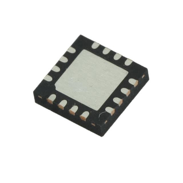
STMicroelectronics M41T93RQA6F
- Part No.:
- M41T93RQA6F
- Manufacturer:
- STMicroelectronics
- Category:
- Real Time Clocks
- Package:
- 16-VQFN Exposed Pad
- Datasheet:
-
 M41T93RQA6F.pdf
- Description:
- IC RTC CLK/CALENDAR SPI 16QFN
- Quantity:
- Payment:

- Shipping:

Inventory:2,737
Please send an inquiry. Send us your inquiry, and we will respond immediately.
Product details
Overview
M41T93RQA6F from STMicroelectronics is a serial SPI real-time clock (RTC) with integrated 32.768 kHz oscillator, battery switchover circuitry, and 7-byte SRAM. It delivers ±5 ppm factory-calibrated accuracy (SOX18), supports 2.7–5.5 V VCC operation, maintains time across power loss using VBAT, and provides alarm, watchdog, 8-bit timer, and programmable 32 kHz square wave output - deployed in industrial control panels requiring long-term timestamp integrity.
For engineers reviewing the M41T93RQA6F datasheet, M41T93RQA6F pinout, M41T93RQA6F application, or M41T93RQA6F equivalent, key selection criteria include backup-mode alarm persistence, analog/digital calibration capability, IRQ/FT/OUT pin interrupt priority in backup mode, and QFN16 package thermal performance under extended temperature cycling.
Technical Context
The M41T93RQA6F implements a fully autonomous RTC subsystem: its embedded oscillator uses either external crystal (QFN16) or factory-mounted crystal (SOX18), with dual-stage calibration-programmable analog load capacitance (0–12.5 pF in 0.5 pF steps) and digital periodic counter correction (±127 ppm adjustment). The device features dedicated hardware for clock data coherency during register reads, preventing partial updates across BCD-formatted time fields.
Its power management includes fixed-reference switchover at VRST = 2.63 V (R variant), automatic write protection during brown-out recovery (tREC = 250 ms min), and oscillator fail detection with interrupt enable. The IRQ/FT/OUT pin operates as open-drain with configurable priority: alarm > watchdog > timer > oscillator fail > frequency test in VCC mode; alarm retains top priority in backup mode.
Key Specifications
| Parameter | Value and Actual Design Meaning |
|---|---|
| Operating Voltage | 2.7 V to 5.5 V on VCC; enables direct interface with 3.3 V microcontrollers without level-shifting. |
| Battery Supply Current | 365 nA typical; extends CR2032 battery life beyond 10 years in backup mode. |
| Accuracy | ±5 ppm typical after two reflows (SOX18); achieved via factory-trimmed analog/digital calibration registers. |
| Temperature Range | –40 °C to +85 °C; validated for industrial automation and outdoor metering environments. |
| SPI Interface | Mode 0 only (CPOL = 0, CPHA = 0); ensures deterministic timing with standard MCU SPI peripherals. |
| Backup Power Source | Voltage switchover at VRST = 2.63 V; guarantees seamless transition to VBAT before system reset. |
| Alarm Capability | Dual programmable alarms with interrupt output active in both VCC and battery modes. |
| User Memory | 7 bytes of battery-backed SRAM; retains configuration or event logs during main power loss. |
Pinout & Package
Package: QFN16, 4 mm × 4 mm, no-lead, wettable flank - optimized for automated optical inspection and thermal dissipation in dense PCB layouts.
| Pin/Terminal | Circuit Role | Design Meaning |
|---|---|---|
| XO | Oscillator output | Drives external 32.768 kHz crystal (QFN16 only); not connected in SOX18 variant. |
| XI | Oscillator input | Accepts crystal feedback signal; internal load capacitance programmable (0–12.5 pF). |
| E | Chip enable | Active-low SPI select; high-Z SDO when E = high; required falling edge initiates all operations. |
| SDI | Serial data input | Latches command/address/data on rising SCL edge; supports 8-bit sequential register access. |
| SDO | Serial data output | Shifts register contents on falling SCL edge; high-impedance when E = high. |
| SCL | Serial clock | Provides synchronous timing; CPOL = 0, CPHA = 0 only - no clock polarity/phase flexibility. |
| IRQ/FT/OUT | Multi-function open-drain output | Delivers alarm/watchdog/timer interrupts; also serves as frequency test point or general-purpose output. |
| RST | Power-on reset output | Open-drain signal asserted low for tREC (250 ms min) after VCC rise above VPFD. |
| SQW | Square wave output | Programmable 32 kHz default; selectable frequencies include 1 Hz, 1.024 kHz, and 4.096 kHz. |
| VBAT | Battery supply input | Connects to coin cell; powers RTC core when VCC < VRST = 2.63 V; includes battery-low flag detection. |
| VCC | Main supply voltage | 2.7–5.5 V operating range; powers digital logic, SPI interface, and calibration circuits. |
| VSS | Ground reference | Common return path for VCC, VBAT, and all I/O; requires low-impedance PCB plane connection. |
Key Features
| Feature | Design Value |
|---|---|
| Dual calibration architecture | Analog (load capacitance trim) + digital (counter offset) correction enables field recalibration without crystal replacement. |
| Backup-mode alarm persistence | Alarm interrupt remains functional even when VCC is absent - critical for unattended logging systems. |
| Hardware clock data coherency | Atomic read mechanism prevents partial BCD register updates during time-of-day reads across second/minute boundaries. |
| Programmable 8-bit countdown timer | Configurable source clock (244.1 μs to 4.25 hrs) and interrupt enable allows flexible event scheduling independent of main CPU. |
| Oscillator fail detection | Dedicated circuit monitors crystal oscillation; asserts interrupt and sets flag within 1 second of stoppage. |
| Century bit support | Two-bit binary-coded century register (CB1:CB0) enables Y2K-compliant date handling through year 2099. |
Applications
| Industrial Data Logger | Smart Energy Meter |
|---|---|
|
Use Scenario: Continuous timestamping of sensor readings during grid outages. IC Role / Device Role / Timing Role: Primary timekeeping and alarm-triggered event capture during VBAT-only operation. Use Value: Maintains accurate UTC-aligned timestamps across multi-day blackouts using 365 nA battery current. |
Use Scenario: Billing-cycle time tracking with tamper-resistant time stamping. IC Role / Device Role / Timing Role: Secure, battery-backed calendar engine with century-bit rollover handling. Use Value: Enables ISO/IEC 62056-compliant billing intervals and leap-year compensation without MCU intervention. |
| Medical Infusion Pump | Building Automation Controller |
|
Use Scenario: Dose scheduling and audit log timestamping with regulatory traceability. IC Role / Device Role / Timing Role: Fail-safe RTC with oscillator fail interrupt and battery-low warning. Use Value: Provides FDA 21 CFR Part 11-compliant time stamps and alerts for maintenance before battery depletion. |
Use Scenario: HVAC schedule execution and occupancy-based lighting control. IC Role / Device Role / Timing Role: Dual-alarm scheduler driving relay outputs and energy reporting cycles. Use Value: Reduces host MCU wake-up frequency by offloading 1 Hz and 24-hour interval timing to hardware timer. |
Equivalent & Alternatives
The following parts are listed as comparable options for similar real-time clock applications.
| Alternative Part | Technical Difference | Application Difference | Selection Advice |
|---|---|---|---|
| DS3231SN#T&R | Integrated TCXO (±2 ppm), higher VCC range (2.3–5.5 V), no analog calibration; 230 nA battery current. | Superior accuracy over temperature; lacks programmable square wave and dual alarms. | Select for precision timing where temperature stability dominates cost and feature requirements. |
| PCF8563T | I²C interface only, no SPI; 0.25 μA battery current; no built-in oscillator - requires external crystal. | Lower pin count and BOM cost; no battery switchover circuitry - requires external power-fail detection. | Select for space-constrained designs with existing I²C infrastructure and minimal accuracy demands. |
Compared with DS3231SN#T&R and PCF8563T, the M41T93RQA6F uniquely balances SPI compatibility, dual-alarm flexibility, and on-chip calibration - making it optimal for industrial systems needing field-adjustable accuracy and deterministic interrupt behavior in mixed-power environments.
Availability
M41T93RQA6F is available at Aetrix Electronics and suitable for industrial data loggers, smart energy meters, medical infusion pumps, and building automation controllers requiring stable component supply across extended product lifecycles.
Supply support for M41T93RQA6F includes scheduled delivery planning, volume procurement assistance, BOM continuity management, traceable sourcing, and lifecycle availability coordination for OEM customers, industrial embedded developers, connected-device designers, and electronics production programs.
Manufacturer
STMicroelectronics is a global semiconductor leader headquartered in Geneva, Switzerland, designing and manufacturing microcontrollers, power ICs, sensors, and timing solutions for industrial, automotive, and consumer markets.
The M41T93 belongs to ST's real-time clock portfolio engineered for high-reliability embedded systems requiring battery-backed timekeeping, deterministic interrupt response, and long-term calibration stability in harsh thermal environments.
FAQ
What is the function of the DU pin on M41T93RQA6F?
The DU (Do Not Use) pin must be tied to VCC per datasheet Figure 3 and Table 1. It is an unused internal test pad with no electrical function; leaving it floating or grounding it may cause undefined behavior or increased leakage current in the QFN16 package.
Does M41T93RQA6F support SPI Mode 3 (CPOL = 1, CPHA = 1)?
No. The M41T93RQA6F supports SPI Mode 0 exclusively (CPOL = 0, CPHA = 0), as confirmed in Section 1.1.3 and Figure 6 of the datasheet. Attempting Mode 3 will result in incorrect data latching on SDI and corrupted SDO output due to mismatched clock edge sampling.
How does the M41T93RQA6F handle leap years and month-end rollovers?
The device automatically adjusts for 28-, 29- (leap year), 30-, and 31-day months using internal BCD arithmetic logic. Leap year calculation follows the Gregorian calendar rule (divisible by 4, except centuries unless divisible by 400), validated across the full –40 °C to +85 °C operating range.
Can the SQW output be disabled or configured to high-impedance state?
No. The SQW pin is a push-pull output with fixed drive strength and no disable control bit. To isolate it, external series resistance or a MOSFET gate driver must be used. The datasheet confirms SQW defaults to 32 kHz on power-up and remains active whenever VCC or VBAT is present.
M41T93RQA6F Specifications
- Product attributes
- Attribute value
- Manufacturer:
- STMicroelectronics
- Series:
- -
- Package/Case:
- 16-VQFN Exposed Pad
- Packaging:
- Tape & Reel (TR)
- Product Status:
- Active
- Programmable:
- Not Verified
- Type:
- Clock/Calendar
- Features:
- Alarm, Leap Year, Square Wave Output, SRAM, Watchdog Timer
- Memory Size:
- 7B
- Time Format:
- HH:MM:SS:hh (24 hr)
- Date Format:
- YY-MM-DD-dd
- Interface:
- SPI
- Voltage - Supply:
- 2.7V ~ 5.5V
- Voltage - Supply, Battery:
- 1.8V ~ 5.5V
- Current - Timekeeping (Max):
- 10µA @ 5.5V
- Operating Temperature:
- -40°C ~ 85°C
- Mounting Type:
- Surface Mount
- Grade:
- -
- Qualification:
- -
- Supplier Device Package:
- 16-QFN (4x4)
M41T93RQA6F FAQ
1.How can I place an order for M41T93RQA6F through Aetrix?
Please submit a Request for Quotation (RFQ) for M41T93RQA6F on Aetrix. Our sales agent will provide a competitive quotation and guide you through the order confirmation once you accept the terms.
2.Are the price and stock information for M41T93RQA6F reliable?
The price and inventory of M41T93RQA6F are updated periodically and may fluctuate due to market conditions. Stock and pricing data are typically refreshed every 24 hours. Quotation validity for M41T93RQA6F is usually 5 days.
3.What payment methods are accepted for M41T93RQA6F?
We accept Wire Transfer, PayPal, Credit Card, Western Union, MoneyGram, and Escrow for M41T93RQA6F transactions.
Note: Certain payment methods may incur a processing fee.
4.How is shipping managed for M41T93RQA6F?
M41T93RQA6F orders can be shipped via leading logistics carriers, including DHL, UPS, FedEx, TNT, or Registered Mail.
Once your M41T93RQA6F order is processed, you will receive an email with the shipment details and tracking number.
Note: Tracking information may take up to 24 hours to appear. Express delivery typically takes 3–5 business days.
5.How can I obtain technical support or documentation for M41T93RQA6F?
For technical support, including M41T93RQA6F datasheets, pinout diagrams, or application guidance, please contact our engineering support team. They can provide detailed documentation and assistance for your M41T93RQA6F requirements.
6.How does Aetrix verify that M41T93RQA6F is sourced from the original manufacturer or authorized distributors?
All M41T93RQA6F products on Aetrix are procured from qualified distributors and authorized channels. Our dedicated quality assurance team conducts strict verification, including traceability checks and, if necessary, third-party testing. This ensures that M41T93RQA6F meets industry standards.
7.What is the process for return or replacement of M41T93RQA6F?
All M41T93RQA6F units undergo pre-shipment inspection (PSI). If there is an issue with M41T93RQA6F, returns or replacements are accepted under the following conditions:
1.Quantity discrepancies, incorrect items, or visible external defects (such as breakage or corrosion), acknowledged by Aetrix.
2.The issue is reported within 90 days of delivery.
3.The M41T93RQA6F part is unused and in its original packaging.
Return procedure for M41T93RQA6F:
1.Submit a request within 90 days.
2.Obtain a Return Material Authorization (RMA) from Aetrix.
M41T93RQA6F Tags

-
MCP7940N-I/SN
Microchip Technology
-
MCP7940MT-I/MNY
Microchip Technology

-
PCF85063ATL/1,118
NXP USA Inc.
-
MCP7940NT-I/SN
Microchip Technology

-
MCP7940NT-I/MS
Microchip Technology
-
MCP7940N-I/MS
Microchip Technology
-
PCF85063AT/AY
NXP USA Inc.

-
PCF85063TP/1Z
NXP Semiconductors

-
PCF85063ATT/AJ
NXP USA Inc.
-
MCP7940NT-E/SN
Microchip Technology
-
MCP7940NT-I/MNY
Microchip Technology
-
MCP79400T-I/SN
Microchip Technology
Tech Hub

A practical engineering and sourcing framework covering lifecycle verification, lifetime-buy calculations, replacement qualification, supplier checks and counterfeit-risk controls.

TTL and CMOS logic families differ in thresholds, loading, output drive, power and timing. This engineering guide compares 74HC and 74HCT, calculates noise margins and checks 3.3 V/5 V compatibility.

A practical engineering guide to 3.3V and 5V logic compatibility, input thresholds, resistor dividers, translator ICs, MOSFET level shifting, I2C pull-ups, timing limits and power-sequencing risks.

The 74HC595 uses push-pull logic outputs, while the TPIC6B595 uses 50 V open-drain DMOS sinks for higher-power loads. This guide compares timing, current limits, 3.3 V interfacing, load wiring, thermal…

The 74HC595 converts serial data into eight stable parallel outputs. This guide covers pin functions, shift and storage timing, OE and MR behavior, drive-current limits, cascading, voltage compatibilit…

A technical comparison of level-sensitive latches and edge-triggered flip-flops, covering timing windows, setup and hold limits, master–slave operation, time borrowing, race-through, HDL inference and…

A D latch stores one bit while Enable controls when data can pass. This reference covers gate-level operation, truth tables, transparency, setup and hold timing, LE versus OE, common ICs and practical …

An SR latch stores one bit through cross-coupled feedback. This engineering reference covers NOR and NAND implementations, truth tables, forbidden-state recovery, gated operation, switch debouncing, fa…

Latch circuits retain one bit through feedback. This technical reference covers SR and D latches, truth tables, transparency, timing limits, latch-versus-flip-flop behavior, applications and common log…

An engineering guide to LED driver operation, constant-current and constant-voltage outputs, linear and switching topologies, dimming, IC selection, calculations, replacement compatibility, and fault c…


