
 My Inquiry
 My Account


STMicroelectronics M48Z35Y-70MH1E
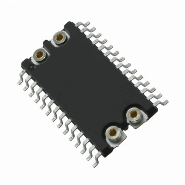
- Part No.:
- M48Z35Y-70MH1E
- Manufacturer:
- STMicroelectronics
- Category:
- Memory
- Package:
- 28-SOP (0.350", 8.89mm Width) with SNAPHAT Sockets
- Datasheet:
-
 M48Z35Y-70MH1E.pdf
- Description:
- IC NVSRAM 256KBIT PARALLEL 28SOH
- Quantity:
- Payment:

- Shipping:

Inventory:1,001
Please send an inquiry. Send us your inquiry, and we will respond immediately.
Product details
Overview
M48Z35Y-70MH1E from STMicroelectronics is a 256 Kbit (32 K × 8) non-volatile ZEROPOWER® SRAM with integrated lithium battery, power-fail detection circuitry, and automatic write protection. It operates at 4.5–5.5 V, features 70 ns read/write cycle time, and retains data for ≥11 years on internal battery during power loss. Used in industrial control panels for real-time parameter storage during brownouts.
For engineers reviewing the M48Z35Y-70MH1E datasheet, M48Z35Y-70MH1E pinout, M48Z35Y-70MH1E application, or M48Z35Y-70MH1E equivalent, key selection criteria include VPFD voltage window (4.2–4.5 V), SOH28 package compatibility with SNAPHAT® top, battery-backed data retention under 0–70 °C, and JEDEC 32K×8 SRAM pin/function equivalence.
Technical Context
The M48Z35Y integrates a 32 K × 8 static RAM array, voltage-sense switching circuitry, and lithium cell management logic on a single die. Its power-fail detection triggers write protection when VCC falls within the 4.2–4.5 V VPFD window and switches to battery backup below 3.0 V (VSO).
It supports standard SRAM timing modes: READ (E low, G low, W high), WRITE (E low, W low), and battery-retention mode (VCC < VSO). All I/Os enter high-impedance state during power fail, and outputs remain undriven until tAVQV (70 ns) after address stabilization under CL = 100 pF.
Key Specifications
| Parameter | Value and Actual Design Meaning |
|---|---|
| Memory size | 256 Kbit (32 K × 8) - provides byte-wide non-volatile storage without EEPROM wear limits |
| Access time | 70 ns - matches JEDEC-standard SRAM timing for drop-in replacement in legacy designs |
| VCC range | 4.5–5.5 V - supports wider supply tolerance than M48Z35 (4.75–5.5 V), easing system-level margining |
| VPFD range | 4.2–4.5 V - lower power-fail threshold enables earlier write protection during gradual brownouts |
| VSO | 3.0 V - switchover voltage at which internal lithium cell powers memory, ensuring data integrity |
| Battery life | ≥11 years at 25 °C - enables long-term unattended operation in metering and logging applications |
| Operating temp | 0–70 °C - qualified for commercial/industrial ambient environments without derating |
Pinout & Package
Package: SOH28 - 28-pin plastic small-outline package with gold-plated contacts for direct mating with SNAPHAT® battery housing (M4Z28-BR00SH1). Designed for surface-mount assembly followed by post-reflow battery attachment.
| Pin/Terminal | Circuit Role | Design Meaning |
|---|---|---|
| A0–A14 | Address inputs | 15-bit address bus supporting full 32 Kbyte addressing; compatible with standard microcontroller address lines |
| DQ0–DQ7 | Data I/O | 8-bit bidirectional data bus with three-state control via E/G; meets TTL/CMOS voltage thresholds |
| E | Chip enable | Active-low chip select; must be held high during VCC ramp-up to prevent inadvertent writes |
| G | Output enable | Active-low output control; used with E to manage bus contention during READ cycles |
| W | Write enable | Active-low write strobe; falling edge initiates WRITE; requires tDVWH = 30 ns data setup before edge |
| VCC | Supply voltage | Primary 4.5–5.5 V power rail; monitored continuously for VPFD/VSO thresholds |
| VSS | Ground | Reference return path for all digital and analog circuitry; decoupling required per Figure 9 |
Key Features
| Feature | Design Value |
|---|---|
| Integrated CAPHAT™/SNAPHAT® battery solution | Eliminates external backup power design; SNAPHAT® mounts post-reflow to avoid thermal damage to Li cell |
| Automatic power-fail write protection | Hardware-enforced write disable within VPFD window (4.2–4.5 V), preventing corruption during brownouts |
| JEDEC 32K×8 pin/function compatibility | Direct socket replacement for standard SRAMs; no PCB redesign or firmware changes needed |
| Zero-power data retention | Internal lithium cell sustains memory contents for ≥11 years at 25 °C with zero external power |
| RoHS-compliant & lead-free | Meets EU environmental directives; SOH28 package uses Pb-free second-level interconnect |
Applications
| Industrial PLC Data Logging | Smart Electricity Meter Parameter Storage |
|---|---|
|
Use Scenario: Retaining calibration coefficients and event logs during utility grid interruptions lasting minutes to hours. IC Role / Device Role / Timing Role: Non-volatile memory buffer that maintains SRAM contents without external backup circuitry or firmware intervention. Use Value: Eliminates need for EEPROM wear leveling or supercapacitor-based backup, reducing BOM count and field failure risk. |
Use Scenario: Preserving tariff schedules, billing registers, and tamper-event timestamps across repeated power cycles. IC Role / Device Role / Timing Role: Pin-compatible SRAM replacement providing guaranteed 11-year data retention on internal battery. Use Value: Meets IEC 62056-21 metering standards for data integrity without external power management ICs. |
| Medical Infusion Pump Configuration Memory | Point-of-Sale Terminal Transaction Buffer |
|
Use Scenario: Storing drug library settings and dose history during battery swaps or AC power loss. IC Role / Device Role / Timing Role: Fail-safe memory element that enters write-protected retention mode before VCC drops below 4.2 V. Use Value: Ensures FDA-required configuration persistence without reliance on host processor or watchdog timers. |
Use Scenario: Holding pending transaction records during brief UPS outages or mains dips in retail kiosks. IC Role / Device Role / Timing Role: High-speed (70 ns) SRAM with automatic switchover to battery at 3.0 V, enabling seamless resume. Use Value: Prevents transaction loss during sub-second power anomalies, satisfying PCI DSS data integrity requirements. |
Equivalent & Alternatives
The following parts are listed as comparable options for similar non-volatile SRAM applications.
| Alternative Part | Technical Difference | Application Difference | Selection Advice |
|---|---|---|---|
| Cypress CY14B101P-BA25XI | 4 Mbit nvSRAM; 25 ns access; separate VCAP capacitor required for backup | Higher density but needs external capacitor and layout space; no integrated battery | Select when >32 KB non-volatility is required and board area allows VCAP placement |
| Renesas R1EX24128ASAS0I | 128 Kbit serial EEPROM; I²C interface; 1 MHz max clock; no SRAM speed or parallel interface | Serial interface only; 5 ms write cycle vs. instant SRAM write; no battery integration | Select only for low-pin-count systems where parallel bus is unavailable and write latency is acceptable |
Compared with CY14B101P-BA25XI and R1EX24128ASAS0I, the M48Z35Y-70MH1E delivers true SRAM speed with zero external components for backup, making it optimal for legacy parallel-bus systems requiring proven 11-year retention without redesign.
Availability
M48Z35Y-70MH1E is available at Aetrix Electronics and suitable for industrial control panels, smart metering systems, and medical device configuration storage requiring stable component supply across multi-year production cycles.
Supply support for M48Z35Y-70MH1E includes scheduled delivery planning, volume procurement assistance, BOM continuity management, traceable sourcing, and lifecycle availability coordination for OEM customers, industrial embedded developers, connected-device designers, and electronics production programs.
Manufacturer
STMicroelectronics is a global semiconductor leader headquartered in Geneva, Switzerland, designing and manufacturing microcontrollers, power management ICs, sensors, and memory solutions for industrial, automotive, and consumer markets.
The M48Z35Y belongs to ST's ZEROPOWER® SRAM product line, engineered specifically to replace volatile SRAMs in systems requiring guaranteed data retention during unpredictable power loss-without external backup components or firmware overhead.
FAQ
What is the purpose of the SNAPHAT® top, and is it included with M48Z35Y-70MH1E?
The SNAPHAT® top (part number M4Z28-BR00SH1) contains a 48 mAh lithium button cell and mounts directly onto the SOH28 package after reflow soldering. It is not included with M48Z35Y-70MH1E-both components are ordered separately per Table 16. This separation prevents battery exposure to soldering temperatures above 125 °C, preserving cell longevity and safety.
How does the M48Z35Y respond to VCC noise or negative transients during battery backup mode?
During battery backup (VCC < VSO), negative VCC undershoots below –0.3 V are strictly prohibited on any pin, as they can corrupt stored data. ST recommends placing a Schottky diode (cathode to VCC, anode to VSS) and a 0.1 µF ceramic bypass capacitor near the device to clamp transients and absorb energy spikes caused by switching or power cycling.
Can M48Z35Y-70MH1E be used as a direct replacement for standard 32K×8 SRAMs like IS61LV25616AL?
Yes-it is pin- and function-compatible with JEDEC-standard 32K×8 SRAMs. Address, data, and control signals (A0–A14, DQ0–DQ7, E, G, W) match exactly. No timing or voltage interface changes are needed. However, VCC must remain within 4.5–5.5 V, and E must be held high during power-up to avoid spurious writes during VPFD recovery.
What is the minimum VCC fall time required to ensure reliable power-fail detection and data retention?
To guarantee write protection activation before data corruption, VCC must fall from VPFD(max) to VPFD(min) in ≥300 µs (tF). Faster drops may delay deselection by up to 200 µs after crossing VPFD(min). For full data retention, VCC must then fall from VPFD(min) to VSS in ≥10 µs (tFB); sub-10 µs transitions risk RAM array corruption.
M48Z35Y-70MH1E Specifications
- Product attributes
- Attribute value
- Manufacturer:
- STMicroelectronics
- Series:
- -
- Package/Case:
- 28-SOP (0.350", 8.89mm Width) with SNAPHAT Sockets
- Packaging:
- Tube
- Product Status:
- Obsolete
- Programmable:
- Not Verified
- Memory Type:
- Non-Volatile
- Memory Format:
- NVSRAM
- Technology:
- NVSRAM (Non-Volatile SRAM)
- Memory Size:
- 256Kbit
- Memory Organization:
- 32K x 8
- Memory Interface:
- Parallel
- Clock Frequency:
- -
- Write Cycle Time - Word, Page:
- 70ns
- Access Time:
- 70 ns
- Voltage - Supply:
- 4.5V ~ 5.5V
- Operating Temperature:
- 0°C ~ 70°C (TA)
- Grade:
- -
- Qualification:
- -
- Mounting Type:
- Surface Mount
- Supplier Device Package:
- 28-SOH
M48Z35Y-70MH1E FAQ
1.How can I place an order for M48Z35Y-70MH1E through Aetrix?
Please submit a Request for Quotation (RFQ) for M48Z35Y-70MH1E on Aetrix. Our sales agent will provide a competitive quotation and guide you through the order confirmation once you accept the terms.
2.Are the price and stock information for M48Z35Y-70MH1E reliable?
The price and inventory of M48Z35Y-70MH1E are updated periodically and may fluctuate due to market conditions. Stock and pricing data are typically refreshed every 24 hours. Quotation validity for M48Z35Y-70MH1E is usually 5 days.
3.What payment methods are accepted for M48Z35Y-70MH1E?
We accept Wire Transfer, PayPal, Credit Card, Western Union, MoneyGram, and Escrow for M48Z35Y-70MH1E transactions.
Note: Certain payment methods may incur a processing fee.
4.How is shipping managed for M48Z35Y-70MH1E?
M48Z35Y-70MH1E orders can be shipped via leading logistics carriers, including DHL, UPS, FedEx, TNT, or Registered Mail.
Once your M48Z35Y-70MH1E order is processed, you will receive an email with the shipment details and tracking number.
Note: Tracking information may take up to 24 hours to appear. Express delivery typically takes 3–5 business days.
5.How can I obtain technical support or documentation for M48Z35Y-70MH1E?
For technical support, including M48Z35Y-70MH1E datasheets, pinout diagrams, or application guidance, please contact our engineering support team. They can provide detailed documentation and assistance for your M48Z35Y-70MH1E requirements.
6.How does Aetrix verify that M48Z35Y-70MH1E is sourced from the original manufacturer or authorized distributors?
All M48Z35Y-70MH1E products on Aetrix are procured from qualified distributors and authorized channels. Our dedicated quality assurance team conducts strict verification, including traceability checks and, if necessary, third-party testing. This ensures that M48Z35Y-70MH1E meets industry standards.
7.What is the process for return or replacement of M48Z35Y-70MH1E?
All M48Z35Y-70MH1E units undergo pre-shipment inspection (PSI). If there is an issue with M48Z35Y-70MH1E, returns or replacements are accepted under the following conditions:
1.Quantity discrepancies, incorrect items, or visible external defects (such as breakage or corrosion), acknowledged by Aetrix.
2.The issue is reported within 90 days of delivery.
3.The M48Z35Y-70MH1E part is unused and in its original packaging.
Return procedure for M48Z35Y-70MH1E:
1.Submit a request within 90 days.
2.Obtain a Return Material Authorization (RMA) from Aetrix.
M48Z35Y-70MH1E Tags

-
M24C02-WMN6TP
STMicroelectronics

-
AT24C02C-XHM-T
Microchip Technology

-
AT21CS01-STUM10-T
Microchip Technology

-
AT24C02C-SSHM-T
Microchip Technology

-
24LC01BT-I/OT
Microchip Technology

-
M24C02-FMC6TG
STMicroelectronics
-
AT24CS02-SSHM-T
Microchip Technology

-
93LC46BT-I/OT
Microchip Technology
-
AT24C04C-SSHM-T
Microchip Technology

-
24LC01BT-I/SN
Microchip Technology
-
24AA02UIDT-I/OT
Microchip Technology

-
AT24C08C-STUM-T
Microchip Technology
Tech Hub

A practical engineering and sourcing framework covering lifecycle verification, lifetime-buy calculations, replacement qualification, supplier checks and counterfeit-risk controls.

TTL and CMOS logic families differ in thresholds, loading, output drive, power and timing. This engineering guide compares 74HC and 74HCT, calculates noise margins and checks 3.3 V/5 V compatibility.

A practical engineering guide to 3.3V and 5V logic compatibility, input thresholds, resistor dividers, translator ICs, MOSFET level shifting, I2C pull-ups, timing limits and power-sequencing risks.

The 74HC595 uses push-pull logic outputs, while the TPIC6B595 uses 50 V open-drain DMOS sinks for higher-power loads. This guide compares timing, current limits, 3.3 V interfacing, load wiring, thermal…

The 74HC595 converts serial data into eight stable parallel outputs. This guide covers pin functions, shift and storage timing, OE and MR behavior, drive-current limits, cascading, voltage compatibilit…

A technical comparison of level-sensitive latches and edge-triggered flip-flops, covering timing windows, setup and hold limits, master–slave operation, time borrowing, race-through, HDL inference and…

A D latch stores one bit while Enable controls when data can pass. This reference covers gate-level operation, truth tables, transparency, setup and hold timing, LE versus OE, common ICs and practical …

An SR latch stores one bit through cross-coupled feedback. This engineering reference covers NOR and NAND implementations, truth tables, forbidden-state recovery, gated operation, switch debouncing, fa…

Latch circuits retain one bit through feedback. This technical reference covers SR and D latches, truth tables, transparency, timing limits, latch-versus-flip-flop behavior, applications and common log…

An engineering guide to LED driver operation, constant-current and constant-voltage outputs, linear and switching topologies, dimming, IC selection, calculations, replacement compatibility, and fault c…


