
 My Inquiry
 My Account


STMicroelectronics M48Z512AY-70PM1
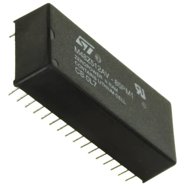
- Part No.:
- M48Z512AY-70PM1
- Manufacturer:
- STMicroelectronics
- Category:
- Memory
- Package:
- 32-DIP Module (0.600", 15.24mm)
- Datasheet:
-
 M48Z512AY-70PM1.pdf
- Description:
- IC NVSRAM 4MBIT PARALLEL 32PMDIP
- Quantity:
- Payment:

- Shipping:

Inventory:2,773
Please send an inquiry. Send us your inquiry, and we will respond immediately.
Product details
Overview
M48Z512AY-70PM1 from STMicroelectronics is a 4 Mbit (512 K × 8) non-volatile ZEROPOWER® SRAM with integrated lithium battery, power-fail detection circuitry, and automatic WRITE protection. It operates as a standard JEDEC-compatible SRAM under VCC (4.5–5.5 V), switches to battery backup when VCC drops below 3.0 V (VSO), and guarantees ≥10 years of data retention without external power. Used in industrial control panels and legacy medical instrumentation for secure real-time parameter storage during brownouts.
For engineers reviewing the M48Z512AY-70PM1 datasheet, M48Z512AY-70PM1 pinout, M48Z512AY-70PM1 application, or M48Z512AY-70PM1 equivalent, key selection criteria include VPFD range (4.2–4.5 V), tAVQV ≤ 70 ns, PMDIP32 package compatibility, and battery-backed data retention without WRITE cycle limits.
Technical Context
The device integrates a CMOS SRAM array, voltage-sense switching circuitry, and a sealed lithium coin cell in a single 32-pin DIP module. Its power-fail logic monitors VCC continuously and initiates WRITE protection within 40–150 µs after crossing VPFD (4.2–4.5 V), then connects the battery at VSO = 3.0 V to sustain memory contents.
It supports conventional asynchronous SRAM timing: READ mode requires E low + W high + G low; WRITE mode requires E and W both active low; all I/O pins enter high-impedance state during power-deselect or battery backup. No special WRITE timing or erase cycles are needed - unlimited WRITE endurance is maintained across both mains-powered and battery-backed operation.
Key Specifications
| Parameter | Value and Actual Design Meaning |
|---|---|
| Memory size | 4,194,304 bits (524,288 × 8); directly replaces standard 512 K × 8 SRAMs without address decoding changes |
| Access time (tAVQV) | 70 ns max; ensures compatibility with 14 MHz bus systems using standard SRAM timing margins |
| VPFD range | 4.2 V to 4.5 V; triggers automatic WRITE protect before system reset threshold is crossed |
| VSO voltage | 3.0 V; switchover point where internal battery assumes power supply to preserve RAM contents |
| Data retention | ≥10 years at 25 °C with no VCC; enabled only after initial VCC application and battery activation |
| Supply current (ICC1 standby) | 10 mA max (TTL E input); enables low-power hold mode while preserving full read/write capability |
| Package | PMDIP32 - 32-pin plastic dual in-line module with ECOPACK® RoHS-compliant lead-free interconnect |
Pinout & Package
PMDIP32 is a 32-pin plastic DIP module with 0.3″ width, 0.1″ pin pitch, and integrated battery cavity. Pin 1 is bottom-left corner (A0), pin 32 is top-right corner (VCC). All pins conform to JEDEC MS-011AC mechanical outline.
| Pin/Terminal | Circuit Role | Design Meaning |
|---|---|---|
| A0–A18 | Address inputs | 19-bit address bus supporting full 524,288-word addressing; TTL/CMOS compatible |
| DQ0–DQ7 | Data I/O bidirectional lines | 8-bit parallel data path; three-state controlled by E and G; no pull-ups required |
| E | Chip enable | Active-low global enable; forces high-Z outputs and disables internal logic when high |
| G | Output enable | Active-low output gate; allows read data to appear on DQ lines independent of write state |
| W | Write enable | Active-low WRITE control; latches data on falling edge; must be coordinated with E for valid writes |
| VCC | Power supply | 4.5–5.5 V nominal; powers SRAM core and control logic; battery disconnects automatically above VSO |
| VSS | Ground reference | System common return; all timing and voltage thresholds referenced to this node |
Key Features
| Feature | Design Value |
|---|---|
| Integrated lithium battery | Sealed, factory-installed coin cell enabling >10-year data retention without external power or charging circuitry |
| Automatic power-fail detection | Detects VCC decay below VPFD (4.2–4.5 V) and asserts WRITE protection within 40–150 µs to prevent corruption |
| JEDEC pin/function compatibility | Direct drop-in replacement for industry-standard 512 K × 8 SRAMs (e.g., AS6C4008, CY62157) |
| Unlimited WRITE cycles | No endurance limitation - same WRITE durability in powered and battery-backed modes due to SRAM architecture |
| ECOPACK® RoHS compliance | PMDIP32 package uses lead-free second-level interconnects and meets EU Directive 2011/65/EU requirements |
Applications
| Industrial PLC Data Logger | Medical Infusion Pump Memory |
|---|---|
|
Use Scenario: Stores calibration coefficients and therapy history during AC power loss or battery swap in Class II medical devices. IC Role / Device Role / Timing Role: Non-volatile SRAM buffer maintaining critical runtime parameters without firmware intervention or EEPROM wear leveling. Use Value: Eliminates need for external backup capacitors or separate NVSRAM controllers; retains data through 100+ power cycles with zero WRITE latency penalty. |
Use Scenario: Holds dosage logs and alarm thresholds in infusion pumps operating in hospital environments with unstable line voltage. IC Role / Device Role / Timing Role: System-level power-fail safeguard ensuring deterministic data preservation during brownouts lasting seconds to minutes. Use Value: Guarantees ≥10-year data integrity without periodic refresh or checksum validation overhead - verified per IEC 62304 clause 5.5.3. |
| Telecom Base Station Clock Buffer | Legacy CNC Machine Parameter Store |
|
Use Scenario: Caches real-time clock registers and sync configuration in outdoor telecom cabinets exposed to wide temperature swings. IC Role / Device Role / Timing Role: Battery-backed SRAM providing glitch-free timekeeping continuity during generator switchover or UPS transition. Use Value: Maintains sub-millisecond timestamp accuracy across power interruptions; avoids NTP re-sync delays or clock drift accumulation. |
Use Scenario: Preserves tool offset tables and axis compensation values in decades-old CNC controllers where firmware updates are prohibited. IC Role / Device Role / Timing Role: Drop-in hardware upgrade replacing obsolete Dallas DS1230Y modules without PCB redesign. Use Value: Enables continued use of legacy control software while meeting modern reliability standards - no change to host microcontroller timing or bus protocol. |
Equivalent & Alternatives
The following parts are listed as comparable options for similar non-volatile SRAM applications.
| Alternative Part | Technical Difference | Application Difference | Selection Advice |
|---|---|---|---|
| AS6C4008-70PCN | Standard 512 K × 8 SRAM (no battery or power-fail logic); 70 ns access; 5 V only; SOJ32 package | Requires external battery + supervisor IC (e.g., MAX690) to achieve comparable data retention | Select only if board space permits discrete backup solution and long-term component availability is prioritized over integration |
| ST M48Z512AV-85PM1 | 3.0–3.6 V operation; VPFD = 2.8–3.0 V; VSO = 2.5 V; same PMDIP32 package; 85 ns access | Designed for 3.3 V systems; lower VPFD enables earlier protection in low-voltage rails but reduces noise margin | Choose when migrating to 3.3 V platforms or when tighter VPFD tolerance is required for brownout resilience |
Compared with AS6C4008-70PCN, M48Z512AY-70PM1 eliminates external supervision components and guarantees 10-year retention out-of-box; versus M48Z512AV-85PM1, it offers faster 70 ns access and higher VPFD margin for 5 V systems, trading off voltage range flexibility.
Availability
M48Z512AY-70PM1 is available at Aetrix Electronics and suitable for industrial PLC data loggers, medical infusion pump memory, telecom base station clock buffers, and legacy CNC machine parameter stores requiring stable component supply amid end-of-life transitions.
Supply support for M48Z512AY-70PM1 includes scheduled delivery planning, volume procurement assistance, BOM continuity management, traceable sourcing, and lifecycle availability coordination for OEM customers, industrial embedded developers, connected-device designers, and electronics production programs.
Manufacturer
STMicroelectronics is a global semiconductor leader headquartered in Geneva, Switzerland, designing and manufacturing analog, MCU, power, and memory solutions for industrial, automotive, and consumer markets.
M48Z512AY-70PM1 belongs to ST's ZEROPOWER® SRAM product line, engineered specifically to replace volatile SRAMs in systems demanding guaranteed data retention during uncontrolled power loss - targeting legacy infrastructure upgrades and safety-critical equipment.
FAQ
Is M48Z512AY-70PM1 recommended for new designs?
No - STMicroelectronics explicitly states "Not recommended for new design" in its official documentation (Doc ID 5146 Rev 9, June 2011). It remains in production for legacy support but lacks roadmap extension. New designs should evaluate modern alternatives like SPI or I²C NVSRAMs or FRAM-based solutions with extended lifecycles.
What is the expected battery lifetime after first power application?
The internal lithium battery provides ≥10 years of data retention at 25 °C after initial VCC application, assuming cumulative time spent in battery backup mode does not exceed that duration. Retention degrades with elevated temperature: at 85 °C, usable life reduces to approximately 2–3 years based on Arrhenius modeling in AN1012.
Can M48Z512AY-70PM1 operate with 3.3 V VCC?
No - the M48Z512AY variant is specified for VCC = 4.5–5.5 V only. Applying 3.3 V violates absolute maximum ratings and will prevent proper power-fail detection (VPFD min = 4.2 V) and SRAM functionality. For 3.3 V systems, use M48Z512AV-85PM1 instead.
Does the device require external bypass capacitance?
Yes - ST recommends a 0.1 µF ceramic capacitor placed between VCC and VSS, as close as possible to the device pins, to suppress switching transients and prevent data corruption during battery backup mode. This is mandatory per Figure 8 and Section 2.4 of the datasheet.
M48Z512AY-70PM1 Specifications
- Product attributes
- Attribute value
- Manufacturer:
- STMicroelectronics
- Series:
- -
- Package/Case:
- 32-DIP Module (0.600", 15.24mm)
- Packaging:
- Tube
- Product Status:
- Obsolete
- Programmable:
- Not Verified
- Memory Type:
- Non-Volatile
- Memory Format:
- NVSRAM
- Technology:
- NVSRAM (Non-Volatile SRAM)
- Memory Size:
- 4Mbit
- Memory Organization:
- 512K x 8
- Memory Interface:
- Parallel
- Clock Frequency:
- -
- Write Cycle Time - Word, Page:
- 70ns
- Access Time:
- 70 ns
- Voltage - Supply:
- 4.5V ~ 5.5V
- Operating Temperature:
- 0°C ~ 70°C (TA)
- Grade:
- -
- Qualification:
- -
- Mounting Type:
- Through Hole
- Supplier Device Package:
- 32-PMDIP Module
M48Z512AY-70PM1 FAQ
1.How can I place an order for M48Z512AY-70PM1 through Aetrix?
Please submit a Request for Quotation (RFQ) for M48Z512AY-70PM1 on Aetrix. Our sales agent will provide a competitive quotation and guide you through the order confirmation once you accept the terms.
2.Are the price and stock information for M48Z512AY-70PM1 reliable?
The price and inventory of M48Z512AY-70PM1 are updated periodically and may fluctuate due to market conditions. Stock and pricing data are typically refreshed every 24 hours. Quotation validity for M48Z512AY-70PM1 is usually 5 days.
3.What payment methods are accepted for M48Z512AY-70PM1?
We accept Wire Transfer, PayPal, Credit Card, Western Union, MoneyGram, and Escrow for M48Z512AY-70PM1 transactions.
Note: Certain payment methods may incur a processing fee.
4.How is shipping managed for M48Z512AY-70PM1?
M48Z512AY-70PM1 orders can be shipped via leading logistics carriers, including DHL, UPS, FedEx, TNT, or Registered Mail.
Once your M48Z512AY-70PM1 order is processed, you will receive an email with the shipment details and tracking number.
Note: Tracking information may take up to 24 hours to appear. Express delivery typically takes 3–5 business days.
5.How can I obtain technical support or documentation for M48Z512AY-70PM1?
For technical support, including M48Z512AY-70PM1 datasheets, pinout diagrams, or application guidance, please contact our engineering support team. They can provide detailed documentation and assistance for your M48Z512AY-70PM1 requirements.
6.How does Aetrix verify that M48Z512AY-70PM1 is sourced from the original manufacturer or authorized distributors?
All M48Z512AY-70PM1 products on Aetrix are procured from qualified distributors and authorized channels. Our dedicated quality assurance team conducts strict verification, including traceability checks and, if necessary, third-party testing. This ensures that M48Z512AY-70PM1 meets industry standards.
7.What is the process for return or replacement of M48Z512AY-70PM1?
All M48Z512AY-70PM1 units undergo pre-shipment inspection (PSI). If there is an issue with M48Z512AY-70PM1, returns or replacements are accepted under the following conditions:
1.Quantity discrepancies, incorrect items, or visible external defects (such as breakage or corrosion), acknowledged by Aetrix.
2.The issue is reported within 90 days of delivery.
3.The M48Z512AY-70PM1 part is unused and in its original packaging.
Return procedure for M48Z512AY-70PM1:
1.Submit a request within 90 days.
2.Obtain a Return Material Authorization (RMA) from Aetrix.
M48Z512AY-70PM1 Tags

-
M24C02-WMN6TP
STMicroelectronics

-
AT24C02C-XHM-T
Microchip Technology

-
AT21CS01-STUM10-T
Microchip Technology

-
AT24C02C-SSHM-T
Microchip Technology

-
24LC01BT-I/OT
Microchip Technology

-
M24C02-FMC6TG
STMicroelectronics
-
AT24CS02-SSHM-T
Microchip Technology

-
93LC46BT-I/OT
Microchip Technology
-
AT24C04C-SSHM-T
Microchip Technology

-
24LC01BT-I/SN
Microchip Technology
-
24AA02UIDT-I/OT
Microchip Technology

-
AT24C08C-STUM-T
Microchip Technology
Tech Hub

A practical engineering and sourcing framework covering lifecycle verification, lifetime-buy calculations, replacement qualification, supplier checks and counterfeit-risk controls.

TTL and CMOS logic families differ in thresholds, loading, output drive, power and timing. This engineering guide compares 74HC and 74HCT, calculates noise margins and checks 3.3 V/5 V compatibility.

A practical engineering guide to 3.3V and 5V logic compatibility, input thresholds, resistor dividers, translator ICs, MOSFET level shifting, I2C pull-ups, timing limits and power-sequencing risks.

The 74HC595 uses push-pull logic outputs, while the TPIC6B595 uses 50 V open-drain DMOS sinks for higher-power loads. This guide compares timing, current limits, 3.3 V interfacing, load wiring, thermal…

The 74HC595 converts serial data into eight stable parallel outputs. This guide covers pin functions, shift and storage timing, OE and MR behavior, drive-current limits, cascading, voltage compatibilit…

A technical comparison of level-sensitive latches and edge-triggered flip-flops, covering timing windows, setup and hold limits, master–slave operation, time borrowing, race-through, HDL inference and…

A D latch stores one bit while Enable controls when data can pass. This reference covers gate-level operation, truth tables, transparency, setup and hold timing, LE versus OE, common ICs and practical …

An SR latch stores one bit through cross-coupled feedback. This engineering reference covers NOR and NAND implementations, truth tables, forbidden-state recovery, gated operation, switch debouncing, fa…

Latch circuits retain one bit through feedback. This technical reference covers SR and D latches, truth tables, transparency, timing limits, latch-versus-flip-flop behavior, applications and common log…

An engineering guide to LED driver operation, constant-current and constant-voltage outputs, linear and switching topologies, dimming, IC selection, calculations, replacement compatibility, and fault c…


