
 My Inquiry
 My Account


Renesas M51660L#TF0J
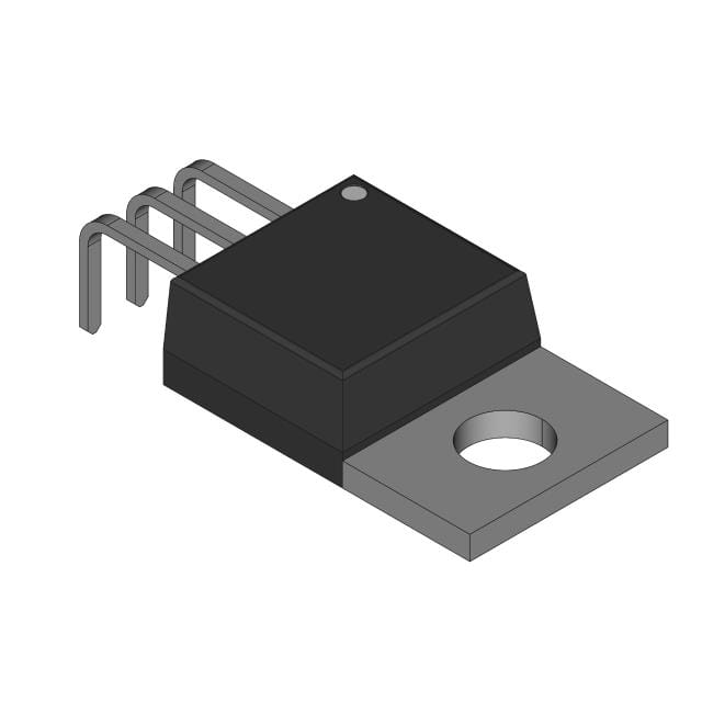
- Part No.:
- M51660L#TF0J
- Manufacturer:
- Renesas
- Category:
- Motor Drivers, Controllers
- Package:
- -
- Datasheet:
-
 M51660L#TF0J.pdf
- Description:
- MIXED SIGNAL SERVO MOTOR CONTROL
- Quantity:
- Payment:

- Shipping:

Inventory:981
Please send an inquiry. Send us your inquiry, and we will respond immediately.
Product details
Overview
M51660L#TF0J from Mitsubishi Electric is a servo motor control IC for radio-controlled (RC) systems, integrating voltage regulation, differential comparator, and dual PNP transistor drive outputs. It operates from 3.5–7 V, delivers 500 mA sink/200 mA source output current, and features 3.5 mA typical circuit current when outputs are off - enabling compact, stable RC servo positioning circuits.
For engineers reviewing the M51660L#TF0J datasheet, M51660L#TF0J pinout, M51660L#TF0J application, or M51660L#TF0J equivalent, key selection considerations include dead band width adjustability (1.5–30 µs), internal 2.6 V regulated supply output, thermal derating (5.5 mW/°C), and compatibility with external 2SA695 PNP transistors in RC servo driver stages.
Technical Context
The M51660L#TF0J implements a triangular-wave timing generator using external R/C networks on pins 2 (timing capacitor) and 3 (timing resistor), feeding a differential comparator that compares servo position voltage (pin 1) against the waveform to generate error pulses. Its internal voltage regulator (pin 12, 2.6 V ±0.15 V) powers internal logic and supports external potentiometer biasing.
Dead band width is set via pin 8 (error pulse output) resistor (RDB = 510 Ω yields 3.4 µs typ.), while pulse stretching is controlled by pin 10 with external R/C. Dual independent output drivers (pins 4 and 11) each sink up to 500 mA and source up to 200 mA to drive external PNP transistors such as 2SA695 in push-pull H-bridge configurations.
Key Specifications
| Parameter | Value and Actual Design Meaning |
|---|---|
| Supply voltage range | 3.5–7 V - supports standard RC battery packs (4.8 V NiCd/NiMH nominal) with margin for voltage sag and ripple. |
| Internal regulated voltage | 2.6 V ±0.15 V - powers internal comparator and reference circuitry, reducing sensitivity to input supply fluctuations. |
| Circuit current (output off) | 3.5 mA typ. - enables low-quiescent-power operation critical for battery-powered RC receivers. |
| Output sink current | 500 mA max - drives base of external PNP transistor (e.g., 2SA695) with sufficient gain for motor coil current switching. |
| Dead band width | 1.5–30 µs adjustable - sets minimum pulse width threshold to prevent servo hunting near center position. |
| Operating temperature | –20 to +75 °C - validated for indoor/outdoor RC use including hobby-grade aircraft and ground vehicles. |
| Thermal derating | 5.5 mW/°C above 25 °C - defines safe power dissipation limit under sustained load in compact enclosures. |
Pinout & Package
Housed in a 14-pin molded plastic zig-zag inline package (ZIP, outline 14P5A), the M51660L#TF0J provides discrete signal routing for RC servo timing, position feedback, and dual-output transistor drive without integrated power switches.
| Pin/Terminal | Circuit Role | Design Meaning |
|---|---|---|
| 1 | Servo position voltage input | Accepts wiper voltage from servo potentiometer; compared against internal triangular wave for position error detection. |
| 2 | Timing capacitor | Connects to external 0.1 µF capacitor to generate linear ramp waveform for PWM timing reference. |
| 3 | Timing resistor | Sets constant-current charging rate (e.g., 18 kΩ → 1.0 mA); determines PWM frequency and resolution. |
| 4 & 11 | External PNP transistor drive | Open-collector outputs driving bases of external PNP transistors (e.g., 2SA695) in complementary motor drive stage. |
| 5 | Input | Accepts positive TTL/CMOS-compatible pulse (≥3 V peak) from RC receiver channel decoder. |
| 6 & 9 | Output (1) / Output (2) | Feedback connection points for timing loop stabilization; tied to pin 2 for oscillator control. |
| 7 & 14 | GND | Dedicated ground terminals - separate return paths reduce noise coupling between analog and digital sections. |
| 8 | Error pulse output | Drives external resistor to set dead band width; higher resistance increases dead zone duration. |
| 10 | Stretcher input | Connects external R/C network to extend pulse width for improved motor torque at low speeds. |
| 12 | Regulated voltage output | 2.6 V reference output - powers potentiometer bias and pulse stretcher components; requires 2.2 µF bypass capacitor. |
| 13 | Supply voltage (VCC) | Primary power input; accepts 3.5–7 V with 10 µF bulk capacitance recommended for transient suppression. |
Key Features
| Feature | Design Value |
|---|---|
| Dual independent PNP drive outputs | Enables full H-bridge motor control using external transistors - avoids need for discrete driver ICs or complex layout. |
| Adjustable dead band width (1.5–30 µs) | Prevents oscillation at neutral position by rejecting small input jitter; set via single external resistor on pin 8. |
| Integrated 2.6 V voltage regulator | Stabilizes internal analog circuitry against supply ripple and temperature drift - eliminates need for external LDO. |
| Protection against continuous "H" level input | Prevents latch-up or overheating during signal loss or receiver timeout - enhances field reliability in RC link dropouts. |
| Low quiescent current (3.5 mA typ.) | Extends battery life in portable RC receivers and micro-servos where standby power budget is constrained. |
Applications
| RC Hobby Servo Positioning | Radio-Controlled Model Aircraft Actuation |
|---|---|
Use Scenario: Precise angular positioning of control surfaces (elevator, rudder, aileron) in 1/10-scale RC cars and aircraft using standard 3-wire PWM interface. IC Role / Device Role / Timing Role: Servo motor controller IC generating direction and duty-cycle-corrected drive signals for external PNP transistor pair. Use Value: Delivers sub-millisecond dead band control and stable 2.6 V internal reference - eliminating center-point jitter and improving repeatability across temperature. | Use Scenario: Driving high-torque metal-geared servos in FPV drone flight controllers where EMI resilience and thermal stability are critical. IC Role / Device Role / Timing Role: Core timing and error-comparison IC in closed-loop position servo system, interfacing RC receiver PWM and potentiometer feedback. Use Value: Supports 500 mA output sink per channel and thermal derating down to –20 °C - ensuring reliable actuator response during cold-weather flight. |
| RC Receiver Integrated Servo Driver | Digital Proportional RC Transmitter Module |
Use Scenario: Embedded servo driver within compact 2.4 GHz RC receiver modules requiring minimal external components and low standby current. IC Role / Device Role / Timing Role: Integrated servo control ASIC providing regulated reference, timing generation, and transistor base drive in single ZIP package. Use Value: Reduces BOM count by integrating voltage regulation and dead band adjustment - cutting PCB area by >30% vs. discrete op-amp + transistor solutions. | Use Scenario: Signal conditioning and pulse shaping stage in programmable RC transmitter modules supporting multiple servo protocols. IC Role / Device Role / Timing Role: Pulse stretcher and error amplifier IC converting microcontroller-generated PWM into robust, noise-immune servo drive signals. Use Value: Adjustable pulse stretch (via pin 10 R/C) and 30 µs max dead band enable protocol flexibility across Futaba, JR, and Spektrum-compatible systems. |
Equivalent & Alternatives
The following parts are listed as comparable options for similar servo motor control applications.
| Alternative Part | Technical Difference | Application Difference | Selection Advice |
|---|---|---|---|
| BA6686F-E2 | Single-output design; no internal voltage regulator; requires external 5 V supply and separate dead band resistor network. | Lacks dual-drive capability and regulated reference - suitable only for simpler, lower-cost RC receivers with fixed supply rails. | Select when board space allows discrete regulation and cost sensitivity outweighs integration benefits. |
| uPC1251C | Higher supply voltage range (4–16 V); no integrated timing capacitor pin; uses external oscillator IC for PWM generation. | Designed for industrial servo amplifiers - lacks RC-specific features like pulse stretcher input and error pulse output. | Choose for wide-input-voltage industrial motion control where RC timing constraints do not apply. |
Compared with BA6686F-E2 and uPC1251C, the M51660L#TF0J uniquely integrates dual PNP drive, internal 2.6 V regulation, and pin-configurable dead band - making it the only option optimized for compact, battery-powered RC servo modules requiring self-contained timing and noise-immune positioning.
Availability
M51660L#TF0J is available at Aetrix Electronics and suitable for RC hobby electronics, model aircraft actuation systems, and digital proportional radio control receivers requiring stable component supply across production volumes and long-lifecycle programs.
Supply support for M51660L#TF0J includes scheduled delivery planning, volume procurement assistance, BOM continuity management, traceable sourcing, and lifecycle availability coordination for OEM customers, industrial embedded developers, connected-device designers, and electronics production programs.
Manufacturer
Mitsubishi Electric Corporation is a Japanese multinational specializing in power systems, industrial automation, and semiconductor solutions, with decades of leadership in analog and mixed-signal ICs for motion control.
The M51660L#TF0J belongs to Mitsubishi's legacy RC servo control IC product line, engineered specifically for high-reliability, low-power, analog-intensive radio control applications where precision timing and thermal stability are essential.
FAQ
What is the function of pin 12 on the M51660L#TF0J?
Pin 12 is the regulated voltage output, delivering a stable 2.6 V ±0.15 V reference used to bias the internal comparator and external potentiometer. The M51660L#TF0J requires a 2.2 µF capacitor between pin 12 and ground for stability. This regulated output eliminates dependency on noisy main supply rails and improves position accuracy across temperature and load variations in the M51660L#TF0J-based servo circuit.
Can the M51660L#TF0J operate from a 3.7 V LiPo battery?
Yes, the M51660L#TF0J supports supply voltages from 3.5 V to 7 V, making it compatible with single-cell 3.7 V LiPo batteries (nominal) and their discharge range (~3.0–4.2 V). At 3.7 V, the M51660L#TF0J maintains full functionality including 500 mA output sink capability and 2.6 V regulated output, provided the 10 µF input capacitor is used to handle transient droop. The M51660L#TF0J's specified 3.5 V minimum ensures reliable startup and operation even at end-of-discharge.
How is dead band width adjusted on the M51660L#TF0J?
Dead band width on the M51660L#TF0J is set by connecting an external resistor between pin 8 (error pulse output) and ground. With CS = 0.1 µF, a 510 Ω resistor yields 3.4 µs typical dead band; increasing resistance extends the width up to 30 µs. This adjustment prevents servo oscillation near neutral position by ignoring small input variations. The M51660L#TF0J's pin 8 configuration allows real-time tuning without changing timing capacitors or firmware - a key advantage in RC field calibration.
Which external transistors are recommended for use with the M51660L#TF0J?
The M51660L#TF0J datasheet specifies 2SA695 PNP transistors for use with its dual drive outputs (pins 4 and 11). These transistors provide adequate gain and saturation characteristics for driving typical RC servo motor coils. The M51660L#TF0J's 500 mA sink capability ensures sufficient base current for 2SA695 devices operating at ≤100 mA collector current. Alternative PNP transistors must match VCEO ≥ 30 V, IC ≥ 150 mA, and hFE > 100 at 10 mA base drive to maintain performance identical to the M51660L#TF0J reference design.
Does the M51660L#TF0J include thermal protection?
The M51660L#TF0J does not include active thermal shutdown circuitry. Instead, it specifies absolute maximum ratings including 550 mW power dissipation at 25 °C and thermal derating of 5.5 mW/°C above that temperature. Designers must ensure heatsinking or airflow limits junction temperature to ≤125 °C. The M51660L#TF0J's low 3.5 mA quiescent current and regulated internal supply reduce self-heating - but sustained 500 mA output sinking requires careful PCB copper area allocation per the M51660L#TF0J thermal derating curve.
M51660L#TF0J Specifications
- Product attributes
- Attribute value
- Manufacturer:
- Renesas
- Series:
- *
- Package/Case:
- -
- Packaging:
- Bulk
- Product Status:
- Active
- Motor Type - Stepper:
- -
- Motor Type - AC, DC:
- -
- Function:
- -
- Output Configuration:
- -
- Interface:
- -
- Technology:
- -
- Step Resolution:
- -
- Applications:
- -
- Current - Output:
- -
- Voltage - Supply:
- -
- Voltage - Load:
- -
- Operating Temperature:
- -
- Grade:
- -
- Qualification:
- -
- Mounting Type:
- -
- Supplier Device Package:
- -
M51660L#TF0J FAQ
1.How can I place an order for M51660L#TF0J through Aetrix?
Please submit a Request for Quotation (RFQ) for M51660L#TF0J on Aetrix. Our sales agent will provide a competitive quotation and guide you through the order confirmation once you accept the terms.
2.Are the price and stock information for M51660L#TF0J reliable?
The price and inventory of M51660L#TF0J are updated periodically and may fluctuate due to market conditions. Stock and pricing data are typically refreshed every 24 hours. Quotation validity for M51660L#TF0J is usually 5 days.
3.What payment methods are accepted for M51660L#TF0J?
We accept Wire Transfer, PayPal, Credit Card, Western Union, MoneyGram, and Escrow for M51660L#TF0J transactions.
Note: Certain payment methods may incur a processing fee.
4.How is shipping managed for M51660L#TF0J?
M51660L#TF0J orders can be shipped via leading logistics carriers, including DHL, UPS, FedEx, TNT, or Registered Mail.
Once your M51660L#TF0J order is processed, you will receive an email with the shipment details and tracking number.
Note: Tracking information may take up to 24 hours to appear. Express delivery typically takes 3–5 business days.
5.How can I obtain technical support or documentation for M51660L#TF0J?
For technical support, including M51660L#TF0J datasheets, pinout diagrams, or application guidance, please contact our engineering support team. They can provide detailed documentation and assistance for your M51660L#TF0J requirements.
6.How does Aetrix verify that M51660L#TF0J is sourced from the original manufacturer or authorized distributors?
All M51660L#TF0J products on Aetrix are procured from qualified distributors and authorized channels. Our dedicated quality assurance team conducts strict verification, including traceability checks and, if necessary, third-party testing. This ensures that M51660L#TF0J meets industry standards.
7.What is the process for return or replacement of M51660L#TF0J?
All M51660L#TF0J units undergo pre-shipment inspection (PSI). If there is an issue with M51660L#TF0J, returns or replacements are accepted under the following conditions:
1.Quantity discrepancies, incorrect items, or visible external defects (such as breakage or corrosion), acknowledged by Aetrix.
2.The issue is reported within 90 days of delivery.
3.The M51660L#TF0J part is unused and in its original packaging.
Return procedure for M51660L#TF0J:
1.Submit a request within 90 days.
2.Obtain a Return Material Authorization (RMA) from Aetrix.
M51660L#TF0J Tags

-
DRV2603RUNR
Texas Instruments

-
DRV8837CDSGR
Texas Instruments

-
DRV8837DSGR
Texas Instruments
-
DRV8838DSGR
Texas Instruments

-
DRV8839DSSR
Texas Instruments

-
EMC2301-1-ACZL-TR
Microchip Technology
-
DRV8231ADSGR
Texas Instruments

-
EMC2302-2-AIZL-TR
Microchip Technology

-
DRV8800PWPR
Texas Instruments
-
DRV8835DSSR
Texas Instruments

-
EMC2303-1-KP-TR
Microchip Technology

-
DRV8876PWPR
Texas Instruments
Tech Hub

A practical engineering and sourcing framework covering lifecycle verification, lifetime-buy calculations, replacement qualification, supplier checks and counterfeit-risk controls.

TTL and CMOS logic families differ in thresholds, loading, output drive, power and timing. This engineering guide compares 74HC and 74HCT, calculates noise margins and checks 3.3 V/5 V compatibility.

A practical engineering guide to 3.3V and 5V logic compatibility, input thresholds, resistor dividers, translator ICs, MOSFET level shifting, I2C pull-ups, timing limits and power-sequencing risks.

The 74HC595 uses push-pull logic outputs, while the TPIC6B595 uses 50 V open-drain DMOS sinks for higher-power loads. This guide compares timing, current limits, 3.3 V interfacing, load wiring, thermal…

The 74HC595 converts serial data into eight stable parallel outputs. This guide covers pin functions, shift and storage timing, OE and MR behavior, drive-current limits, cascading, voltage compatibilit…

A technical comparison of level-sensitive latches and edge-triggered flip-flops, covering timing windows, setup and hold limits, master–slave operation, time borrowing, race-through, HDL inference and…

A D latch stores one bit while Enable controls when data can pass. This reference covers gate-level operation, truth tables, transparency, setup and hold timing, LE versus OE, common ICs and practical …

An SR latch stores one bit through cross-coupled feedback. This engineering reference covers NOR and NAND implementations, truth tables, forbidden-state recovery, gated operation, switch debouncing, fa…

Latch circuits retain one bit through feedback. This technical reference covers SR and D latches, truth tables, transparency, timing limits, latch-versus-flip-flop behavior, applications and common log…

An engineering guide to LED driver operation, constant-current and constant-voltage outputs, linear and switching topologies, dimming, IC selection, calculations, replacement compatibility, and fault c…


