
 My Inquiry
 My Account


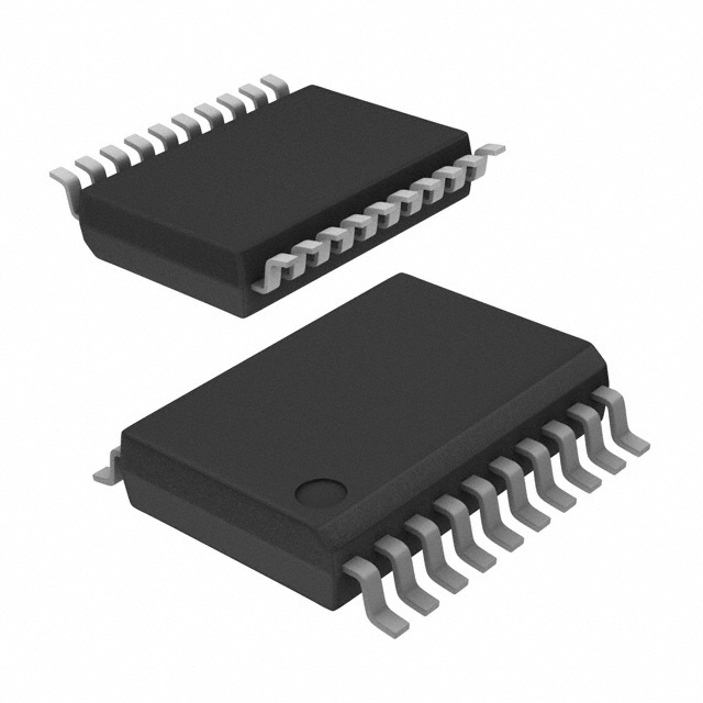
Analog Devices Inc./Maxim Integrated MAX14001AAP+
- Part No.:
- MAX14001AAP+
- Manufacturer:
- Analog Devices Inc./Maxim Integrated
- Category:
- Analog to Digital Converters (ADC)
- Package:
- 20-SSOP (0.209", 5.30mm Width)
- Datasheet:
-
 MAX14001AAP+.pdf
- Description:
- IC ADC 10BIT SAR 20SSOP
- Quantity:
- Payment:

- Shipping:

Inventory:202
Please send an inquiry. Send us your inquiry, and we will respond immediately.
Product details
Overview
The MAX14001AAP+ from Maxim Integrated is a configurable, isolated 10-bit analog-to-digital converter with integrated programmable voltage comparators, inrush current control, and isolated DC-DC power for binary input conditioning. It delivers 3.75kVRMS isolation, 10ksps ADC throughput, <150µs comparator response (unfiltered), and supports 12V–300V high-voltage binary inputs in industrial digital input modules.
For engineers reviewing the MAX14001AAP+ datasheet, MAX14001AAP+ pinout, MAX14001AAP+ application, or MAX14001AAP+ equivalent, this device serves as a single-chip solution for isolated multi-range binary sensing-enabling field-side diagnostics, programmable wetting pulses, noise-rejecting bias current, and SPI-configurable thresholds without external isolators or power supplies.
Technical Context
The MAX14001AAP+ integrates a SAR-based 10-bit ADC, dual-threshold magnitude comparator, isolated DC-DC converter (VDDF output), and two current DACs-one for programmable bias current (50µA–3.75mA) and one for programmable inrush current (50µA–105mA, 0–120ms). All field-side circuitry operates autonomously using the internal isolated supply, enabling diagnostics even with no input signal.
It implements a daisy-chainable 5MHz SPI interface for register configuration, real-time ADC data readout (filtered/unfiltered), and fault reporting via open-drain FAULT pin. The comparator output (COUT) responds to AIN voltage relative to THU/THL thresholds, with latency dependent on filter depth (2/4/8-sample moving average) and mode (voltage-triggered or FAST).
Key Specifications
| Parameter | Value and Actual Design Meaning |
|---|---|
| Isolation Rating | 3.75kVRMS for 60s (UL1577 certified); enables safe interfacing to 300V field-side inputs. |
| ADC Resolution & Speed | 10-bit SAR; 10ksps nominal throughput; provides sufficient resolution for ±0.5% full-scale binary threshold detection. |
| Comparator Latency | <150µs (unfiltered); ensures rapid binary state detection critical for contact bounce mitigation in relay monitoring. |
| Bias Current Range | Programmable 50µA–3.75mA (0.25mA steps); balances capacitive noise rejection against power dissipation in high-impedance inputs. |
| Inrush Current Control | Programmable magnitude (7mA steps) and duration (8ms steps); cleans relay contacts during closure without external timing circuitry. |
| SPI Interface | 5MHz max clock; daisy-chainable; supports real-time register access, fault flag reading, and dual ADC data streams (filtered/unfiltered). |
| Package | 20-pin SSOP; 5.5mm creepage/clearance; Group II CTI material; meets IEC 60112 tracking requirements for industrial environments. |
Pinout & Package
MAX14001AAP+ uses a 20-pin SSOP package (7.9mm × 7.33mm) with 5.5mm minimum creepage and clearance, rated for Group II CTI (Comparative Tracking Index >400), suitable for pollution degree 2 and climatic category 40/125/21.
| Pin/Terminal | Circuit Role | Design Meaning |
|---|---|---|
| VDDL | Logic-side power supply | 1.71V–5.5V input powering SPI interface, registers, and comparator logic; requires local 10µF||1000pF bypass to GNDL. |
| VDD | Isolated DC-DC primary supply | 3.0V–3.6V input powering the internal isolated DC-DC converter; enables field-side operation independent of input signal presence. |
| GNDL / GNDF | Logic- and field-side grounds | Galvanically separated ground domains; mandatory physical separation prevents isolation barrier compromise. |
| AIN / AGND | Analog input reference pair | AIN measures 0–1.25V differential to AGND; supports resistor-divider scaling for 12V–300V input range. |
| ISET | Bias/inrush current reference | Connect 120kΩ resistor to GNDF to set precision current reference; parasitic capacitance must be <10pF for accuracy. |
| GATE / IFET | High-voltage FET gate drive & current sink | GATE supplies gate bias to external depletion-mode FET; IFET sinks programmable inrush/bias current from FET source. |
| COUT | Digital comparator output | Open-drain logic-level output indicating AIN status vs. THU/THL thresholds; directly interfaces to microcontroller GPIO. |
| CS / SCLK / SDI / SDO | SPI interface signals | Standard 4-wire SPI (MOSI/MISO) with chip select; supports daisy-chaining multiple devices on shared bus. |
| FAULT | Diagnostic fault indicator | Open-drain active-low output latching conditions like UVLO, ADC error, or isolation fault; cleared via SPI register write. |
Key Features
| Feature | Design Value |
|---|---|
| Integrated Isolated DC-DC Converter | Provides regulated VDDF output to power field-side ADC, comparators, and DACs-enabling diagnostics with zero input voltage. |
| Programmable Inrush Pulse Generator | Configurable magnitude (50µA–105mA) and duration (0–120ms) eliminates need for external pulse generators in relay contact cleaning. |
| Dual-Mode Input Bias Control | Adjustable 50µA–3.75mA bias current reduces capacitive noise coupling while minimizing power loss in high-impedance binary inputs. |
| Filter-Selectable ADC Output | Simultaneous access to unfiltered (low-latency) and filtered (noise-reduced) 10-bit readings via SPI-supports both fast response and stable decision logic. |
| Field-Side Self-Diagnostics | Automatic verification of ADC functionality, reference stability, and isolation integrity without host intervention-reducing system maintenance overhead. |
Applications
| Distribution Automation | Substation Automation |
|---|---|
|
Use Scenario: Monitoring AC line voltage presence across multiple feeders in medium-voltage switchgear. IC Role / Device Role / Timing Role: Isolated binary input conditioner converting 120V–300V AC-derived DC signals into clean, noise-immune logic-level outputs for PLC or RTU input cards. Use Value: Eliminates external optocouplers and isolated power supplies while providing programmable wetting pulses to prevent contact oxidation in electromechanical relays. |
Use Scenario: Detecting breaker status and auxiliary contact closures in GIS (Gas-Insulated Switchgear) control panels. IC Role / Device Role / Timing Role: High-voltage binary sensor with field-side diagnostics, enabling predictive maintenance by verifying input path integrity before fault events occur. Use Value: Reduces false alarms from EMI-induced transients through programmable filtering and bias current optimization for long cable runs. |
| Industrial Digital Input Modules | Multi-Range Binary Sensing Systems |
|
Use Scenario: Compact DIN-rail mounted I/O modules requiring individually isolated 24V/48V/120V/240V inputs per channel. IC Role / Device Role / Timing Role: Channel-level isolated ADC + comparator + FET driver, supporting mixed-voltage inputs without external level-shifting or isolation components. Use Value: Cuts BOM count by 40% versus discrete isolation solutions and enables per-channel programmability for flexible factory-floor deployment. |
Use Scenario: Retrofitting legacy machinery with modern binary input capability across varying supply voltages (e.g., 12V sensors to 230V AC lines). IC Role / Device Role / Timing Role: Configurable front-end that scales input range via external resistor dividers while maintaining consistent 10-bit resolution and threshold accuracy. Use Value: Enables single hardware design to support global voltage standards-reducing inventory SKUs and qualification effort. |
Equivalent & Alternatives
The following parts are listed as comparable options for similar isolated binary input conditioning applications.
| Alternative Part | Technical Difference | Application Difference | Selection Advice |
|---|---|---|---|
| MAX14002AAP+ | Fixed inrush current (49mA/48ms); no voltage-triggered mode; identical pinout, ADC, comparator, and bias current features. | Best suited for cost-sensitive designs where programmable inrush is unnecessary and FAST-mode-only operation is acceptable. | Select MAX14002AAP+ when simplified configuration and lower unit cost outweigh need for inrush customization. |
| ADI AD7403BRIZ-RL | 2nd-order sigma-delta modulator + digital filter; no integrated DC-DC, no inrush/bias DACs; requires external isolated power and comparator logic. | Requires additional components for full binary input functionality; used where ultra-high noise immunity (>20-bit effective resolution) is prioritized over integration. | Choose AD7403BRIZ-RL only when system already includes isolated power and needs higher-resolution modulation-not as a drop-in replacement. |
Compared with MAX14002AAP+, the MAX14001AAP+ adds full inrush configurability and voltage-triggered activation, enabling adaptive contact cleaning; compared with AD7403BRIZ-RL, it delivers complete signal chain integration-including isolated power, conditioning, and actuation-reducing board area and validation scope.
Availability
MAX14001AAP+ is available at Aetrix Electronics and suitable for distribution automation, substation monitoring, and industrial digital input modules requiring stable component supply, long-term lifecycle support, and UL-certified isolation performance.
Supply support for MAX14001AAP+ includes scheduled delivery planning, volume procurement assistance, BOM continuity management, traceable sourcing, and lifecycle availability coordination for OEM customers, industrial embedded developers, connected-device designers, and electronics production programs.
Manufacturer
Maxim Integrated, now part of Analog Devices, designs high-performance analog and mixed-signal ICs for industrial, automotive, and communications systems-with emphasis on integration, reliability, and safety compliance.
The MAX14001AAP+ belongs to Maxim's isolated binary input ADC family, engineered specifically for high-density, multi-range digital input modules needing galvanic isolation, self-diagnostics, and programmable contact conditioning in harsh electrical environments.
FAQ
What is the maximum input voltage range supported by the MAX14001AAP+?
The MAX14001AAP+ itself accepts 0V–1.25V at its AIN pin, but with an external resistor divider, it supports field-side input voltages from 12V to 300V DC. The device's 3.75kVRMS isolation rating and 5.5mm creepage ensure safe operation at these levels when properly laid out per IEC 61000-4-5 surge and IEC 60664-1 insulation coordination standards. The MAX14001AAP+ does not directly sense high voltage-it conditions scaled-down representations with calibrated accuracy.
How does the MAX14001AAP+ enable field-side diagnostics without an external power source?
The MAX14001AAP+ integrates an isolated DC-DC converter powered by VDD (3.0V–3.6V logic supply), generating VDDF to power all field-side circuitry-including the ADC, comparators, and current DACs-even when no input signal is present. This allows continuous self-tests, reference validation, and leakage checks on the field side independent of the binary input voltage, a capability confirmed in the device's functional description and typical operating characteristics.
Can the MAX14001AAP+ drive standard N-channel MOSFETs for inrush control?
No-the MAX14001AAP+ is designed to drive external depletion-mode high-voltage FETs (e.g., IXTY08N100D2), not enhancement-mode N-channel MOSFETs. Its GATE pin provides a buffered ~3.6V bias referenced to GNDF, insufficient to fully enhance most N-channel devices at high drain voltages. The datasheet explicitly specifies depletion-mode FET usage and includes gate drive capacitor recommendations (0.01µF to GNDF) aligned with depletion-mode gate characteristics.
What is the difference between voltage-triggered and FAST inrush modes in the MAX14001AAP+?
Voltage-triggered mode initiates inrush when the ADC reading crosses the INRT threshold; FAST mode triggers inrush as soon as the external FET can sink current-bypassing ADC conversion delay. Voltage mode enables precise voltage-based contact closure detection, while FAST mode offers minimal latency for time-critical applications. Only the MAX14001AAP+ supports both; the MAX14002AAP+ is FAST-mode only, as stated in the "High-Voltage FET Current Control" section.
Does the MAX14001AAP+ support external voltage references, and what are the limitations?
Yes-the MAX14001AAP+ supports both internal (1.25V ±5%) and external references via the REFIN pin. External references may be series-type (powered from VDDF) or shunt-type (powered by internal 70µA current source), but must draw ≤70µA total. Series references require 0.1µF bypass to AGND; shunt types connect directly between REFIN and AGND. Configuration is done via CFG register bits EXRF and EXTI, as defined in Table 1 of the datasheet.
MAX14001AAP+ Specifications
- Product attributes
- Attribute value
- Manufacturer:
- Analog Devices Inc./Maxim Integrated
- Series:
- -
- Package/Case:
- 20-SSOP (0.209", 5.30mm Width)
- Packaging:
- Tube
- Product Status:
- Active
- Number of Bits:
- 10
- Sampling Rate (Per Second):
- 10k
- Number of Inputs:
- 1
- Input Type:
- Single Ended
- Data Interface:
- SPI
- Configuration:
- S/H-ADC
- Ratio - S/H:ADC:
- 1:1
- Number of A/D Converters:
- 1
- Architecture:
- SAR
- Reference Type:
- External, Internal
- Voltage - Supply, Analog:
- 3V ~ 3.6V
- Voltage - Supply, Digital:
- 1.71V ~ 5.5V
- Features:
- -
- Operating Temperature:
- -40°C ~ 125°C
- Supplier Device Package:
- 20-SSOP
- Mounting Type:
- Surface Mount
- Grade:
- -
- Qualification:
- -
MAX14001AAP+ FAQ
1.How can I place an order for MAX14001AAP+ through Aetrix?
Please submit a Request for Quotation (RFQ) for MAX14001AAP+ on Aetrix. Our sales agent will provide a competitive quotation and guide you through the order confirmation once you accept the terms.
2.Are the price and stock information for MAX14001AAP+ reliable?
The price and inventory of MAX14001AAP+ are updated periodically and may fluctuate due to market conditions. Stock and pricing data are typically refreshed every 24 hours. Quotation validity for MAX14001AAP+ is usually 5 days.
3.What payment methods are accepted for MAX14001AAP+?
We accept Wire Transfer, PayPal, Credit Card, Western Union, MoneyGram, and Escrow for MAX14001AAP+ transactions.
Note: Certain payment methods may incur a processing fee.
4.How is shipping managed for MAX14001AAP+?
MAX14001AAP+ orders can be shipped via leading logistics carriers, including DHL, UPS, FedEx, TNT, or Registered Mail.
Once your MAX14001AAP+ order is processed, you will receive an email with the shipment details and tracking number.
Note: Tracking information may take up to 24 hours to appear. Express delivery typically takes 3–5 business days.
5.How can I obtain technical support or documentation for MAX14001AAP+?
For technical support, including MAX14001AAP+ datasheets, pinout diagrams, or application guidance, please contact our engineering support team. They can provide detailed documentation and assistance for your MAX14001AAP+ requirements.
6.How does Aetrix verify that MAX14001AAP+ is sourced from the original manufacturer or authorized distributors?
All MAX14001AAP+ products on Aetrix are procured from qualified distributors and authorized channels. Our dedicated quality assurance team conducts strict verification, including traceability checks and, if necessary, third-party testing. This ensures that MAX14001AAP+ meets industry standards.
7.What is the process for return or replacement of MAX14001AAP+?
All MAX14001AAP+ units undergo pre-shipment inspection (PSI). If there is an issue with MAX14001AAP+, returns or replacements are accepted under the following conditions:
1.Quantity discrepancies, incorrect items, or visible external defects (such as breakage or corrosion), acknowledged by Aetrix.
2.The issue is reported within 90 days of delivery.
3.The MAX14001AAP+ part is unused and in its original packaging.
Return procedure for MAX14001AAP+:
1.Submit a request within 90 days.
2.Obtain a Return Material Authorization (RMA) from Aetrix.
MAX14001AAP+ Tags
-
ADC081C021CIMKX/NOPB
Texas Instruments

-
MCP3021A5T-E/OT
Microchip Technology
-
TLA2024IRUGR
Texas Instruments
-
MCP3221A5T-E/OT
Microchip Technology
-
MCP3221A5T-I/OT
Microchip Technology
-
MCP3221A4T-E/OT
Microchip Technology
-
MCP3221A6T-E/OT
Microchip Technology
-
MCP3221A0T-E/OT
Microchip Technology
-
MCP3221A1T-E/OT
Microchip Technology

-
ADC121S021CIMFX/NOPB
Texas Instruments

-
MCP3001-I/MS
Microchip Technology

-
MCP3001-I/SN
Microchip Technology
Tech Hub

A practical engineering guide to 3.3V and 5V logic compatibility, input thresholds, resistor dividers, translator ICs, MOSFET level shifting, I2C pull-ups, timing limits and power-sequencing risks.

The 74HC595 uses push-pull logic outputs, while the TPIC6B595 uses 50 V open-drain DMOS sinks for higher-power loads. This guide compares timing, current limits, 3.3 V interfacing, load wiring, thermal…

The 74HC595 converts serial data into eight stable parallel outputs. This guide covers pin functions, shift and storage timing, OE and MR behavior, drive-current limits, cascading, voltage compatibilit…

A technical comparison of level-sensitive latches and edge-triggered flip-flops, covering timing windows, setup and hold limits, master–slave operation, time borrowing, race-through, HDL inference and…

A D latch stores one bit while Enable controls when data can pass. This reference covers gate-level operation, truth tables, transparency, setup and hold timing, LE versus OE, common ICs and practical …

An SR latch stores one bit through cross-coupled feedback. This engineering reference covers NOR and NAND implementations, truth tables, forbidden-state recovery, gated operation, switch debouncing, fa…

Latch circuits retain one bit through feedback. This technical reference covers SR and D latches, truth tables, transparency, timing limits, latch-versus-flip-flop behavior, applications and common log…

An engineering guide to LED driver operation, constant-current and constant-voltage outputs, linear and switching topologies, dimming, IC selection, calculations, replacement compatibility, and fault c…

Operational amplifier guide covering op amp basics, feedback, ideal vs real op amps, common configurations, buffer circuits, offset, bias current, gain-bandwidth, slew rate, rail-to-rail limits and sel…

Jumper cables guide covering safe connection order, red and black clamp placement, final ground connection, cable gauge, length, clamp quality, copper vs CCA cables, jump starter comparison and battery…


