
 My Inquiry
 My Account


Analog Devices Inc./Maxim Integrated MAX14750AEWA+
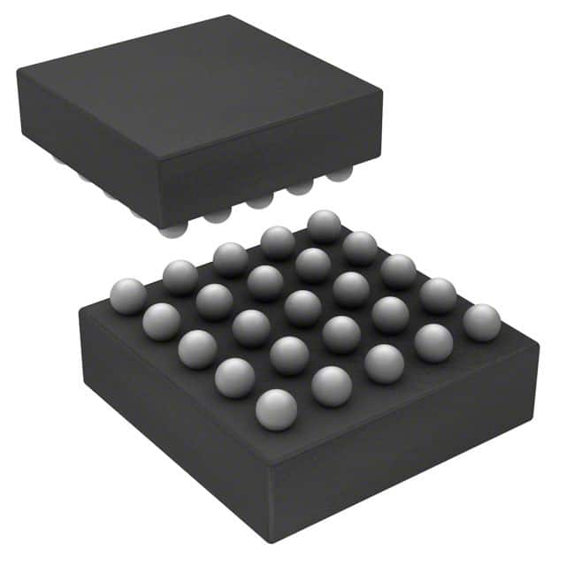
- Part No.:
- MAX14750AEWA+
- Manufacturer:
- Analog Devices Inc./Maxim Integrated
- Category:
- Voltage Regulators - Linear + Switching
- Package:
- 25-WFBGA, WLBGA
- Datasheet:
-
 MAX14750AEWA+.pdf
- Description:
- IC REG TRIPLE BUCK/BST/LNR 25WLP
- Quantity:
- Payment:

- Shipping:

Inventory:1,866
Please send an inquiry. Send us your inquiry, and we will respond immediately.
Product details
Overview
MAX14750AEWA+ from Analog Devices is a highly integrated, micro-IQ power-management IC designed as a companion PMIC for rechargeable battery systems. It integrates a 250mW buck-boost regulator (2.5V–5V output), a 200mA synchronous buck regulator (1.0V–2.0V), a 100mA LDO (0.9V–4.0V), and a 200mA load switch with battery monitoring - all in a 25-bump WLP (2.26mm × 2.14mm). It enables flexible, pin-controlled sequencing in wearable medical and fitness devices.
For engineers reviewing the MAX14750AEWA+ datasheet, MAX14750AEWA+ pinout, MAX14750AEWA+ application, or MAX14750AEWA+ equivalent, this page delivers verified electrical specs, I²C interface behavior, thermal shutdown thresholds, battery impedance measurement capability, and direct enable-pin control architecture - critical for low-power, space-constrained portable designs.
Technical Context
The MAX14750AEWA+ implements independent hardware enable inputs (HVEN, SWEN, LEN, BEN) for each regulator and switch, eliminating reliance on internal sequencers - unlike the MAX14720. Its buck-boost and buck regulators operate in burst mode at light loads, achieving 1.1µA and 0.9µA quiescent current respectively, while supporting programmable current limits and soft-start timing.
Battery impedance measurement is disabled in the MAX14750AEWA+, as confirmed by device-specific functional partitioning in the datasheet; only the MAX14720 includes BatZUVLO and SWOUT-based impedance detection. The monitor multiplexer (MON pin) supports voltage sampling across HVIN, BIN, SWOUT, LOUT, and BOUT with ≤500Ω switch resistance and 80µs break-before-make timing.
Key Specifications
| Parameter | Value and Actual Design Meaning |
|---|---|
| Buck-Boost Output | 2.5V to 5.0V programmable in 100mV steps; supports display biasing and wide-input battery rails |
| Buck Regulator Output | 1.0V to 2.0V programmable in 25mV steps; optimized for low-voltage digital cores |
| LDO Output | 0.9V to 4.0V programmable in 100mV steps; configurable as load switch with 1Ω RON at 1.8V |
| Quiescent Current | 0.9µA (LDO), 0.9µA (buck), 1.1µA (buck-boost); enables multi-year shelf life in sealed wearables |
| Switch On-Resistance | 250mΩ max at 2.7V; supports 200mA continuous load with <67mV dropout |
| Operating Temp Range | −40°C to +85°C; qualified for clinical-grade wearable environments |
| I²C Interface | Standard-mode (400kHz) with open-drain SDA/SCL; supports register read/write for dynamic configuration |
Pinout & Package
MAX14750AEWA+ uses a 25-bump, 0.4mm pitch wafer-level package (WLP), measuring 2.26mm × 2.14mm. The bump layout is defined per JEDEC MO-220, outline 21-0788, with RoHS-compliant finish indicated by the '+' suffix.
| Pin/Terminal | Circuit Role | Design Meaning |
|---|---|---|
| HVEN | Buck-Boost Enable | Active-high hardware control; bypasses I²C for deterministic startup |
| SWEN | Power Switch Enable | Direct gate control of 200mA load switch; enables battery isolation during sleep |
| LEN | LDO Enable | Active-high input; allows LDO to be used as programmable power rail or load disconnect switch |
| BEN | Buck Regulator Enable | Hardware-triggered activation; decouples sequencing from firmware dependencies |
| MON | Multiplexer Output | Single-pin analog readback of HVIN/BIN/SWOUT/LOUT/BOUT via internal switches |
| SCL/SDA | I²C Interface | Configurable registers for voltage setpoints, UVLO thresholds, discharge modes, and timing |
| VCC | Supply Input | Primary bias rail (1.8V–5.5V); powers internal logic and I²C interface |
| SWIN/SWOUT | Load Switch Terminals | Isolates battery from system loads; supports impedance measurement only on MAX14720 (not enabled here) |
Key Features
| Feature | Design Value |
|---|---|
| Independent Hardware Enables | Four dedicated pins (HVEN, SWEN, LEN, BEN) allow asynchronous, firmware-independent power control |
| Micro-IQ Burst Mode | 1.1µA (buck-boost) and 0.9µA (buck/LDO) quiescent current extend battery runtime in standby |
| Programmable Output Voltages | All three regulators support fine-grained digital programming - 100mV (HVOUT/LOUT), 25mV (BOUT) steps |
| Monitor Multiplexer | Single MON pin samples five voltage nodes with <500Ω switch resistance and 80µs BBM timing |
| Thermal Protection | 150°C shutdown with 21°C hysteresis per regulator block ensures safe operation under sustained load |
Applications
| Wearable Medical Sensors | Portable ECG Monitors |
|---|---|
Use Scenario: Continuous biosignal acquisition in patch-style cardiac monitors powered by single-cell Li-ion batteries. IC Role / Device Role / Timing Role: Provides isolated, low-noise 1.8V rail for ADC and 3.3V for BLE radio via independent buck and LDO; load switch isolates battery during deep sleep. Use Value: 0.9µA LDO quiescent current and 250mΩ switch RON reduce sleep-mode drain to <2.8µA total, enabling >3-year battery life. | Use Scenario: Battery-powered, FDA-cleared ECG device requiring clinical-grade voltage stability and rapid wake-up. IC Role / Device Role / Timing Role: Delivers tightly regulated 2.5V for analog front-end and 1.2V for microcontroller core using buck-boost and buck regulators with burst-mode efficiency. Use Value: ±3% output accuracy and <31mV load transient response ensure ECG signal integrity during motion-induced current surges. |
| Fitness Tracker Power Hub | Smart Hearing Aid Subsystem |
Use Scenario: Multi-rail wearable with optical HR sensor, accelerometer, and Bluetooth LE transceiver sharing one coin-cell or small Li-po. IC Role / Device Role / Timing Role: Buck-boost supplies 3.3V to BLE radio, buck supplies 1.1V to MCU, LDO supplies 2.8V to sensor; all enabled independently via GPIOs. Use Value: Pin-controlled enables eliminate I²C boot dependency, reducing wake latency to <100ms for motion-triggered sensing. | Use Scenario: Miniaturized hearing aid with ultra-low-power DSP, MEMS microphone, and rechargeable microbattery. IC Role / Device Role / Timing Role: Powers DSP core (1.0V buck), RF section (2.5V buck-boost), and analog bias (3.0V LDO); load switch disconnects battery during charging. Use Value: 2.26mm × 2.14mm WLP footprint fits within 5mm × 5mm PCB area constraints while delivering 250mW boost capability. |
Equivalent & Alternatives
The following parts are listed as comparable options for similar power-management applications.
| Alternative Part | Technical Difference | Application Difference | Selection Advice |
|---|---|---|---|
| MAX14720AEWA+ | Includes push-button sequencer, battery impedance measurement, seal mode (120nA), and POR delay; lacks independent enable pins | Optimized for non-rechargeable or removable-battery systems requiring ultra-low-off-state current and shipping-mode control | Select MAX14720AEWA+ when button-driven power sequencing and sub-µA off-state are required; not pin-compatible due to different enable pin mapping |
| TPS65218D0RSLR | Quad DC/DC + LDO PMIC with integrated charger; larger 48-ball QFN; no battery impedance monitor; higher IQ (5µA) | Targeted at embedded AM335x/AM437x processors; includes USB/AC charger path and fuel gauge interface | Choose TPS65218D0RSLR for processor-centric designs needing integrated charging; MAX14750AEWA+ offers superior micro-IQ and smaller WLP for wearables |
Compared with MAX14720AEWA+, the MAX14750AEWA+ trades sequencer automation and battery seal mode for deterministic pin-control flexibility - making it ideal for rechargeable systems where firmware manages sequencing. Against TPS65218D0RSLR, it delivers 5× lower quiescent current and 60% smaller footprint, but lacks charger integration.
Availability
MAX14750AEWA+ is available at Aetrix Electronics and suitable for wearable medical sensors, portable ECG monitors, and fitness tracker power hubs requiring stable component supply, long-term lifecycle support, and validated wafer-level packaging performance.
Supply support for MAX14750AEWA+ includes scheduled delivery planning, volume procurement assistance, BOM continuity management, traceable sourcing, and lifecycle availability coordination for OEM customers, industrial embedded developers, connected-device designers, and electronics production programs.
Manufacturer
Analog Devices, Inc. is a global leader in high-performance analog, mixed-signal, and digital signal processing semiconductors, headquartered in Wilmington, MA.
The MAX147xx family targets ultra-low-power, space-constrained portable electronics - specifically engineered to replace discrete power solutions in wearables, medical patches, and IoT edge nodes where microamp quiescent current and sub-3mm² footprint are mandatory.
FAQ
What is the primary functional distinction between MAX14750AEWA+ and MAX14720AEWA+?
The MAX14750AEWA+ provides individual hardware enable pins (HVEN, SWEN, LEN, BEN) for direct, firmware-independent control of each regulator and switch, whereas the MAX14720AEWA+ uses an internal sequencer with push-button monitoring and automatic power-on sequencing. Battery impedance measurement and seal mode (120nA) are exclusive to MAX14720AEWA+. Both share identical regulators and WLP packaging, but pin functions differ - MAX14750AEWA+ does not support BatZUVLO or KIN/KOUT button logic.
Does MAX14750AEWA+ support battery impedance measurement like the MAX14720AEWA+?
No, battery impedance measurement is not supported in the MAX14750AEWA+. This feature is explicitly documented as exclusive to the MAX14720AEWA+ in the datasheet's "Battery Impedance Measurement (MAX14720, BatZUVLO Enabled Only)" section. The MAX14750AEWA+ omits the BatZUVLO function and associated SWOUT-based measurement circuitry, aligning with its role as a companion PMIC rather than a primary battery manager.
What are the absolute maximum ratings for the SWIN and SWOUT pins of MAX14750AEWA+?
The absolute maximum rating for SWIN is −0.3V to +6.0V; for SWOUT, it is −0.3V to (VBIN + 0.3V). Continuous current into SWIN is rated at ±1000mA, while SWOUT supports up to 200mA continuous output. These ratings are specified in the "Absolute Maximum Ratings" table of the MAX14750AEWA+ datasheet and apply across the full −40°C to +85°C operating temperature range.
Can the LDO in MAX14750AEWA+ be configured as a load switch, and what is its on-resistance?
Yes, the LDO in MAX14750AEWA+ can be configured as a load switch via register control. In switch mode, its on-resistance is 1Ω at VLIN = 1.8V and ILOUT = 50mA, and 3Ω at VLIN = 1.2V and ILOUT = 5mA. This dual-mode operation (regulator or switch) is confirmed in the Electrical Characteristics table under "Switch Mode Resistance (RON_LDO)" and enables flexible power routing without external FETs.
What is the thermal shutdown behavior of the buck-boost regulator in MAX14750AEWA+?
Each regulator block in MAX14750AEWA+ has independent thermal protection. The buck-boost regulator triggers shutdown at TJ = 150°C with 21°C hysteresis (TSHDN_BST and TSHDN_HYST_BST). Upon shutdown, the regulator disables switching, holds HVOUT in high-impedance state, and asserts no system-wide reset - allowing other blocks (e.g., buck, LDO) to remain operational if undamaged. Recovery occurs automatically once junction temperature falls below 129°C.
MAX14750AEWA+ Specifications
- Product attributes
- Attribute value
- Manufacturer:
- Analog Devices Inc./Maxim Integrated
- Series:
- -
- Package/Case:
- 25-WFBGA, WLBGA
- Packaging:
- Strip
- Product Status:
- Active
- Topology:
- Step-Down (Buck) (1), Step-Down/Step-Up (Buck/Boost) (1), Linear (LDO) (1)
- Number of Outputs:
- 3
- Frequency - Switching:
- 2MHz
- Voltage/Current - Output 1:
- 2.5V ~ 5V, PROG
- Voltage/Current - Output 2:
- 1V ~ 2V, 250mA
- Voltage/Current - Output 3:
- 0.9V ~ 4V, 100mA
- w/LED Driver:
- No
- w/Supervisor:
- No
- w/Sequencer:
- No
- Voltage - Supply:
- 1.8V ~ 5.5V
- Operating Temperature:
- -40°C ~ 85°C
- Grade:
- -
- Qualification:
- -
- Mounting Type:
- Surface Mount
- Supplier Device Package:
- 25-WLP (2.11x2.23)
MAX14750AEWA+ FAQ
1.How can I place an order for MAX14750AEWA+ through Aetrix?
Please submit a Request for Quotation (RFQ) for MAX14750AEWA+ on Aetrix. Our sales agent will provide a competitive quotation and guide you through the order confirmation once you accept the terms.
2.Are the price and stock information for MAX14750AEWA+ reliable?
The price and inventory of MAX14750AEWA+ are updated periodically and may fluctuate due to market conditions. Stock and pricing data are typically refreshed every 24 hours. Quotation validity for MAX14750AEWA+ is usually 5 days.
3.What payment methods are accepted for MAX14750AEWA+?
We accept Wire Transfer, PayPal, Credit Card, Western Union, MoneyGram, and Escrow for MAX14750AEWA+ transactions.
Note: Certain payment methods may incur a processing fee.
4.How is shipping managed for MAX14750AEWA+?
MAX14750AEWA+ orders can be shipped via leading logistics carriers, including DHL, UPS, FedEx, TNT, or Registered Mail.
Once your MAX14750AEWA+ order is processed, you will receive an email with the shipment details and tracking number.
Note: Tracking information may take up to 24 hours to appear. Express delivery typically takes 3–5 business days.
5.How can I obtain technical support or documentation for MAX14750AEWA+?
For technical support, including MAX14750AEWA+ datasheets, pinout diagrams, or application guidance, please contact our engineering support team. They can provide detailed documentation and assistance for your MAX14750AEWA+ requirements.
6.How does Aetrix verify that MAX14750AEWA+ is sourced from the original manufacturer or authorized distributors?
All MAX14750AEWA+ products on Aetrix are procured from qualified distributors and authorized channels. Our dedicated quality assurance team conducts strict verification, including traceability checks and, if necessary, third-party testing. This ensures that MAX14750AEWA+ meets industry standards.
7.What is the process for return or replacement of MAX14750AEWA+?
All MAX14750AEWA+ units undergo pre-shipment inspection (PSI). If there is an issue with MAX14750AEWA+, returns or replacements are accepted under the following conditions:
1.Quantity discrepancies, incorrect items, or visible external defects (such as breakage or corrosion), acknowledged by Aetrix.
2.The issue is reported within 90 days of delivery.
3.The MAX14750AEWA+ part is unused and in its original packaging.
Return procedure for MAX14750AEWA+:
1.Submit a request within 90 days.
2.Obtain a Return Material Authorization (RMA) from Aetrix.
MAX14750AEWA+ Tags

-
TPS6521905RHBR
Texas Instruments
-
MIC3385YHL-TR
Microchip Technology
-
A4402ELPTR-T
Allegro MicroSystems

-
LM26480SQ-AA/NOPB
Texas Instruments
-
A4402KLPTR-T
Allegro MicroSystems
-
BD71847AMWV-E2
ROHM Semiconductor
-
ADP5040ACPZ-1-R7
Analog Devices Inc.
-
LT3048IDC#TRPBF
Analog Devices Inc.
-
ADP5037ACPZ-R7
Analog Devices Inc.

-
XRP7714ILB-F
MaxLinear, Inc.
-
LTC3260EDE#TRPBF
Analog Devices Inc.
-
LTC3260EMSE#PBF
Analog Devices Inc.
Tech Hub

A practical engineering guide to 3.3V and 5V logic compatibility, input thresholds, resistor dividers, translator ICs, MOSFET level shifting, I2C pull-ups, timing limits and power-sequencing risks.

The 74HC595 uses push-pull logic outputs, while the TPIC6B595 uses 50 V open-drain DMOS sinks for higher-power loads. This guide compares timing, current limits, 3.3 V interfacing, load wiring, thermal…

The 74HC595 converts serial data into eight stable parallel outputs. This guide covers pin functions, shift and storage timing, OE and MR behavior, drive-current limits, cascading, voltage compatibilit…

A technical comparison of level-sensitive latches and edge-triggered flip-flops, covering timing windows, setup and hold limits, master–slave operation, time borrowing, race-through, HDL inference and…

A D latch stores one bit while Enable controls when data can pass. This reference covers gate-level operation, truth tables, transparency, setup and hold timing, LE versus OE, common ICs and practical …

An SR latch stores one bit through cross-coupled feedback. This engineering reference covers NOR and NAND implementations, truth tables, forbidden-state recovery, gated operation, switch debouncing, fa…

Latch circuits retain one bit through feedback. This technical reference covers SR and D latches, truth tables, transparency, timing limits, latch-versus-flip-flop behavior, applications and common log…

An engineering guide to LED driver operation, constant-current and constant-voltage outputs, linear and switching topologies, dimming, IC selection, calculations, replacement compatibility, and fault c…

Operational amplifier guide covering op amp basics, feedback, ideal vs real op amps, common configurations, buffer circuits, offset, bias current, gain-bandwidth, slew rate, rail-to-rail limits and sel…

Jumper cables guide covering safe connection order, red and black clamp placement, final ground connection, cable gauge, length, clamp quality, copper vs CCA cables, jump starter comparison and battery…


