
 My Inquiry
 My Account


Analog Devices Inc./Maxim Integrated MAX14906ATM+
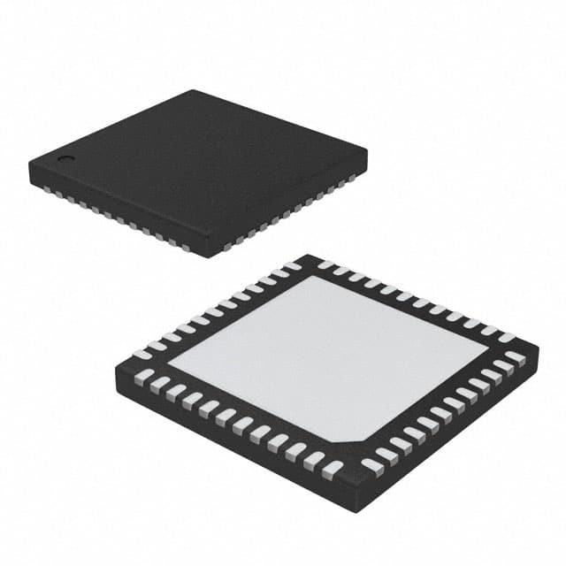
- Part No.:
- MAX14906ATM+
- Manufacturer:
- Analog Devices Inc./Maxim Integrated
- Category:
- Specialized
- Package:
- 48-WFQFN Exposed Pad
- Datasheet:
-
 MAX14906ATM+.pdf
- Description:
- QUAD INDUSTRIAL DIGITAL INPUT /
- Quantity:
- Payment:

- Shipping:

Inventory:928
Please send an inquiry. Send us your inquiry, and we will respond immediately.
Product details
Overview
The MAX14906ATM+ from Analog Devices is a quad-channel, IEC 61131-2-compliant industrial digital I/O device configurable per channel as high-side switch (120mΩ typical RON), push-pull driver, or Type 1/3 or Type 2 digital input with 2.3mA/7mA current sinks. It operates from 10V to 40V supply (65V tolerant) and delivers 0.6µs DO / 1µs DI propagation delay for PLC and motor control applications.
For engineers reviewing the MAX14906ATM+ datasheet, MAX14906ATM+ pinout, MAX14906ATM+ application, or MAX14906ATM+ equivalent, key selection factors include per-channel mode configurability (HS/PP/DI), programmable current limiting (130mA–1.2A), integrated diagnostics (open-wire, short-to-VDD, thermal shutdown), and SPI-addressable multi-device operation in compact 48-pin TQFN.
Technical Context
The MAX14906ATM+ implements independent per-channel configuration via SPI registers and direct logic pins (D1–D4, SYNCH), supporting simultaneous high-speed output updates or input sampling on falling SYNCH edge. Its architecture integrates four isolated DOI_ channels, each with dedicated gate drivers (G1–G4), active clamps for inductive load demagnetization, and dual-supply monitoring (VDD/VDD_ overvoltage lockout at 43.5V, undervoltage warning at 14V).
Diagnostics are hardware-accelerated: open-wire detection uses configurable test currents (20–760µA) and threshold voltage (5.8V), while short-to-VDD detection offers four selectable thresholds (8.2–15V). The device embeds a 5-bit CRC SPI interface, watchdog timer (200–1200ms timeout), and LED matrix (L1–L4, FLED, SLED) for real-time per-channel status and fault indication.
Key Specifications
| Parameter | Value and Actual Design Meaning |
|---|---|
| Supply Range | 10V to 40V VDD/VDD_, 65V absolute max - enables robust operation in 24V industrial systems with surge margin. |
| High-Side RON | 120mΩ typical at 25°C - minimizes power loss and heat rise at 1A output current. |
| Current Limit Range | 130mA to 1.2A (settable via CL_[1:0]) with 2× inrush option - supports diverse solenoid, relay, and indicator loads. |
| Propagation Delay | 0.6µs (DO low-to-high), 1.1µs (DI low-to-high) - ensures deterministic timing for high-speed I/O cycle control. |
| Digital Input Sink | 2.3mA (Type 1/3) or 7mA (Type 2) - meets IEC 61131-2 voltage threshold and hysteresis requirements. |
| ESD/Surge Rating | ±16kV air-gap / ±8kV contact ESD; ±1kV IEC 61000-4-5 surge (with TVS on VDD) - satisfies industrial EMC immunity standards. |
| Operating Temp | −40°C to +125°C junction - qualified for extended deployment in harsh cabinet and field environments. |
Pinout & Package
The MAX14906ATM+ is housed in a 48-pin, 7mm × 7mm TQFN package (package code T4877+6C) with exposed pad (EP) for thermal management. Pin layout supports symmetric power distribution: five VDD-related pins (VDD, VDD1–VDD4), four PGND pins, and dedicated GND for logic integrity.
| Pin/Terminal | Circuit Role | Design Meaning |
|---|---|---|
| VDD, VDD1–VDD4 | Channel-specific power supplies | Enable independent sourcing per DOI_ channel; VDD_ can be individually regulated or shared with local 1µF bypassing. |
| DOI1–DOI4 (dual pins each) | Configurable I/O terminals | Each pair (e.g., DOI1 pins 15/16) serves as high-side output, push-pull driver, or digital input sink - no external components required. |
| D1–D4, SYNCH, EN | Direct logic interface | Allow real-time, non-SPI I/O state control and synchronization - eliminates protocol latency for time-critical updates. |
| G1–G4 | Gate drivers for external pMOS | Support reverse-current protection and full IEC 61131-2 Type 2 compliance when external FETs are used on VDD_ lines. |
| L1–L4, FLED, SLED, VLED | LED driver matrix outputs | Provide per-channel status (L1–L4), fault (FLED), and system status (SLED) indication using common-anode topology with external current-setting resistors. |
| CS, SDI, SDO, CLK, A0/A1 | Addressable SPI interface | Enable daisy-chaining up to four devices on one bus using 2-bit hardware address (A1/A0); CRCEN optional for error detection. |
Key Features
| Feature | Design Value |
|---|---|
| Per-channel mode configurability | Each of four DOI_ channels independently set as HS switch, active-clamp PP, simple PP, or DI (Type 1/3 or Type 2) - eliminates need for multiple discrete I/O ICs. |
| Integrated diagnostics engine | Hardware-accelerated open-wire, short-to-VDD, thermal overload, and supply UV/OV detection - reduces host MCU firmware overhead and improves system reliability. |
| SafeDemag™ active clamp | Unlimited inductive demagnetization energy handling without snubbers - enables safe, fast turn-off of high-inductance solenoids and valves. |
| On-chip 5V LDO (V5) | Internal regulator delivers up to 25mA at 5.0V (±2.5%) - powers logic interface and external circuitry, reducing external BOM count. |
| Robust EMC design | ±16kV air-gap ESD on DOI_ pins and ±1kV surge tolerance (with single TVS on VDD) - simplifies PCB-level protection and certification effort. |
Applications
| PLC Digital I/O Module | Industrial Motor Starter Control |
|---|---|
|
Use Scenario: Modular backplane I/O card in programmable logic controller rack handling 24V DC field signals. IC Role / Device Role / Timing Role: Quad-channel configurable I/O transceiver managing discrete actuator commands and sensor feedback with synchronized state updates via SYNCH. Use Value: Eliminates separate HI/LO-side drivers and DI conditioners; 0.6µs DO propagation enables sub-millisecond scan cycles in safety-rated motion control. |
Use Scenario: Compact motor starter unit controlling contactor coils and monitoring auxiliary contacts in HVAC or pump systems. IC Role / Device Role / Timing Role: High-side switch for 24V coil drive with active clamp and real-time open-load detection on each output. Use Value: Prevents coil burnout from broken wiring; SafeDemag™ allows immediate de-energization without voltage spikes - meets IEC 60947-4-1 requirements. |
| Distributed I/O Node | Factory Automation Safety Interface |
|
Use Scenario: Remote I/O node on PROFINET or EtherNet/IP network collecting machine status and issuing valve commands. IC Role / Device Role / Timing Role: Configurable digital input/output hub with SPI diagnostics reporting and LED status per channel for field maintenance. Use Value: Reduces wiring complexity by consolidating 4 inputs + 4 outputs into one IC; open-wire detection cuts troubleshooting time during commissioning. |
Use Scenario: Safety-rated emergency stop (E-stop) monitor interfacing dual-channel mechanical switches to safety PLC. IC Role / Device Role / Timing Role: Dual redundant Type 2 digital input with independent current sinks and short-to-VDD detection on both channels. Use Value: Meets PL e / SIL 2 requirements via hardware-based diagnostics; 7mA sink ensures reliable switching across temperature and cable length variations. |
Equivalent & Alternatives
The following parts are listed as comparable options for similar industrial digital I/O applications.
| Alternative Part | Technical Difference | Application Difference | Selection Advice |
|---|---|---|---|
| MAX14905ATM+ | 3-channel version, identical architecture and pinout except missing DOI4/G4/L4 - shares same register map and diagnostics. | Suitable for space-constrained 3-I/O designs; not drop-in for 4-channel layouts due to pin count reduction. | Select when BOM consolidation across 3- and 4-channel variants is prioritized; software compatibility simplifies firmware reuse. |
| ADuM1401BRWZ | Quad-channel digital isolator only - no power switching, no diagnostics, no current regulation; requires external drivers and sensing. | Used in isolation barrier only; cannot replace MAX14906ATM+'s integrated power I/O function. | Choose only as companion isolator upstream of MAX14906ATM+ - never as functional substitute for direct field connection. |
Compared with MAX14905ATM+, the MAX14906ATM+ adds a fourth fully featured channel without increasing footprint; versus ADuM1401BRWZ, it delivers complete signal conditioning, power delivery, and diagnostics in one package - eliminating six or more discrete components in typical PLC output stage designs.
Availability
MAX14906ATM+ is available at Aetrix Electronics and suitable for industrial PLC modules, distributed I/O nodes, and motor control starters requiring stable component supply, long-term lifecycle support, and guaranteed RoHS-compliant manufacturing.
Supply support for MAX14906ATM+ includes scheduled delivery planning, volume procurement assistance, BOM continuity management, traceable sourcing, and lifecycle availability coordination for OEM customers, industrial embedded developers, connected-device designers, and electronics production programs.
Manufacturer
Analog Devices, Inc. is a global leader in high-performance analog, mixed-signal, and digital signal processing semiconductors, serving industrial, automotive, communications, and healthcare markets.
The MAX14906ATM+ belongs to Analog Devices' industrial interface portfolio, designed specifically for ruggedized, diagnostics-rich digital I/O in programmable controllers, safety systems, and factory automation equipment.
FAQ
What is the maximum supply voltage the MAX14906ATM+ can tolerate?
The MAX14906ATM+ has an absolute maximum rating of +65V on VDD and all VDD_ pins, with normal operation specified from 10V to 40V. This 65V tolerance provides robust surge headroom for industrial 24V systems subject to load-dump transients. Operation above 40V is not recommended for continuous use, as internal overvoltage lockout triggers at 43.5V (typical) to protect downstream circuitry. The MAX14906ATM+ remains functional and undamaged within its absolute ratings, but sustained overvoltage may trigger shutdown or degrade long-term reliability.
Can the MAX14906ATM+ drive both digital outputs and inputs simultaneously on different channels?
Yes, the MAX14906ATM+ supports true per-channel configuration: any combination of high-side switch, push-pull driver, or Type 1/3 or Type 2 digital input can be active concurrently across its four DOI_ channels. Configuration is controlled via SPI registers (SetOUT, ConfigDO, ConfigDI) or hardware pins (EN, SYNCH), and modes persist independently per channel after power-up. This flexibility allows a single MAX14906ATM+ to serve as both output driver for actuators and input conditioner for sensors in compact industrial nodes - no reconfiguration delay or shared resource contention occurs.
How does open-wire detection work on the MAX14906ATM+ and what is its accuracy?
Open-wire detection on the MAX14906ATM+ applies a programmable diagnostic test current (20–760µA, selected via OWOffCs bits) to the DOI_ pin while the channel is off, then measures resulting voltage. Detection triggers when voltage exceeds 5.8V (typical threshold). The feature works only in off-state and supports four sensitivity levels to accommodate varying cable capacitance and leakage. Accuracy is ensured by on-chip reference trimming - VTH_OWOFF is guaranteed 5.0V to 5.8V over temperature - enabling reliable identification of broken wires or disconnected loads without external components.
Does the MAX14906ATM+ require external components for basic operation?
The MAX14906ATM+ operates with minimal external components: only decoupling capacitors (1µF on VDD/VDD_, 0.1µF on VL, 1µF on V5) are mandatory. Optional components include a TVS diode on VDD for ±1kV surge protection, pull-up resistors on FAULT/VDDOK (to V5 or VL), and current-limiting resistors on L1–L4 LEDs. External pMOS FETs on VDD_ lines are needed only for full IEC 61131-2 Type 2 compliance or reverse-current blocking. No external current-sense resistors, snubbers, or level shifters are required - the MAX14906ATM+ integrates all core functions on-die.
What is the role of the G1–G4 pins on the MAX14906ATM+?
The G1–G4 pins on the MAX14906ATM+ are gate drivers for external pMOS transistors placed between VDD_ and the DOI_ output. They enable reverse-current protection and ensure full IEC 61131-2 Type 2 digital input compliance by actively clamping the input node during off-state. When unused, G1–G4 may be left unconnected - the MAX14906ATM+ functions fully as a high-side or push-pull driver without them. Their inclusion allows designers to meet stringent industrial immunity standards while retaining flexibility to simplify the bill of materials where lower-tier compliance suffices.
MAX14906ATM+ Specifications
- Product attributes
- Attribute value
- Manufacturer:
- Analog Devices Inc./Maxim Integrated
- Series:
- -
- Package/Case:
- 48-WFQFN Exposed Pad
- Packaging:
- Tray
- Product Status:
- Active
- Applications:
- PLC Digital Input Modules
- Interface:
- SPI
- Voltage - Supply:
- 10V ~ 40V
- Supplier Device Package:
- 48-TQFN (7x7)
- Grade:
- -
- Qualification:
- -
- Mounting Type:
- Surface Mount
MAX14906ATM+ FAQ
1.How can I place an order for MAX14906ATM+ through Aetrix?
Please submit a Request for Quotation (RFQ) for MAX14906ATM+ on Aetrix. Our sales agent will provide a competitive quotation and guide you through the order confirmation once you accept the terms.
2.Are the price and stock information for MAX14906ATM+ reliable?
The price and inventory of MAX14906ATM+ are updated periodically and may fluctuate due to market conditions. Stock and pricing data are typically refreshed every 24 hours. Quotation validity for MAX14906ATM+ is usually 5 days.
3.What payment methods are accepted for MAX14906ATM+?
We accept Wire Transfer, PayPal, Credit Card, Western Union, MoneyGram, and Escrow for MAX14906ATM+ transactions.
Note: Certain payment methods may incur a processing fee.
4.How is shipping managed for MAX14906ATM+?
MAX14906ATM+ orders can be shipped via leading logistics carriers, including DHL, UPS, FedEx, TNT, or Registered Mail.
Once your MAX14906ATM+ order is processed, you will receive an email with the shipment details and tracking number.
Note: Tracking information may take up to 24 hours to appear. Express delivery typically takes 3–5 business days.
5.How can I obtain technical support or documentation for MAX14906ATM+?
For technical support, including MAX14906ATM+ datasheets, pinout diagrams, or application guidance, please contact our engineering support team. They can provide detailed documentation and assistance for your MAX14906ATM+ requirements.
6.How does Aetrix verify that MAX14906ATM+ is sourced from the original manufacturer or authorized distributors?
All MAX14906ATM+ products on Aetrix are procured from qualified distributors and authorized channels. Our dedicated quality assurance team conducts strict verification, including traceability checks and, if necessary, third-party testing. This ensures that MAX14906ATM+ meets industry standards.
7.What is the process for return or replacement of MAX14906ATM+?
All MAX14906ATM+ units undergo pre-shipment inspection (PSI). If there is an issue with MAX14906ATM+, returns or replacements are accepted under the following conditions:
1.Quantity discrepancies, incorrect items, or visible external defects (such as breakage or corrosion), acknowledged by Aetrix.
2.The issue is reported within 90 days of delivery.
3.The MAX14906ATM+ part is unused and in its original packaging.
Return procedure for MAX14906ATM+:
1.Submit a request within 90 days.
2.Obtain a Return Material Authorization (RMA) from Aetrix.
MAX14906ATM+ Tags

-
NVT4857UKAZ
NXP Semiconductors

-
TCA8418RTWR
Texas Instruments

-
PCA9546APWR
Texas Instruments

-
MD0100N8-G
Microchip Technology

-
PCA9548APW,118
NXP Semiconductors

-
PCA9540BDP,118
NXP Semiconductors

-
PCA9548APWR
Texas Instruments

-
PCA9546APW,118
NXP Semiconductors

-
PTN3360DBS,518
NXP Semiconductors

-
PCA9546ABS,118
NXP Semiconductors

-
PCA9518PWR
Texas Instruments

-
PCA9545APW,118
NXP Semiconductors
Tech Hub

A practical engineering guide to 3.3V and 5V logic compatibility, input thresholds, resistor dividers, translator ICs, MOSFET level shifting, I2C pull-ups, timing limits and power-sequencing risks.

The 74HC595 uses push-pull logic outputs, while the TPIC6B595 uses 50 V open-drain DMOS sinks for higher-power loads. This guide compares timing, current limits, 3.3 V interfacing, load wiring, thermal…

The 74HC595 converts serial data into eight stable parallel outputs. This guide covers pin functions, shift and storage timing, OE and MR behavior, drive-current limits, cascading, voltage compatibilit…

A technical comparison of level-sensitive latches and edge-triggered flip-flops, covering timing windows, setup and hold limits, master–slave operation, time borrowing, race-through, HDL inference and…

A D latch stores one bit while Enable controls when data can pass. This reference covers gate-level operation, truth tables, transparency, setup and hold timing, LE versus OE, common ICs and practical …

An SR latch stores one bit through cross-coupled feedback. This engineering reference covers NOR and NAND implementations, truth tables, forbidden-state recovery, gated operation, switch debouncing, fa…

Latch circuits retain one bit through feedback. This technical reference covers SR and D latches, truth tables, transparency, timing limits, latch-versus-flip-flop behavior, applications and common log…

An engineering guide to LED driver operation, constant-current and constant-voltage outputs, linear and switching topologies, dimming, IC selection, calculations, replacement compatibility, and fault c…

Operational amplifier guide covering op amp basics, feedback, ideal vs real op amps, common configurations, buffer circuits, offset, bias current, gain-bandwidth, slew rate, rail-to-rail limits and sel…

Jumper cables guide covering safe connection order, red and black clamp placement, final ground connection, cable gauge, length, clamp quality, copper vs CCA cables, jump starter comparison and battery…


