
 My Inquiry
 My Account


Analog Devices Inc./Maxim Integrated MAX16046ETN+CK9
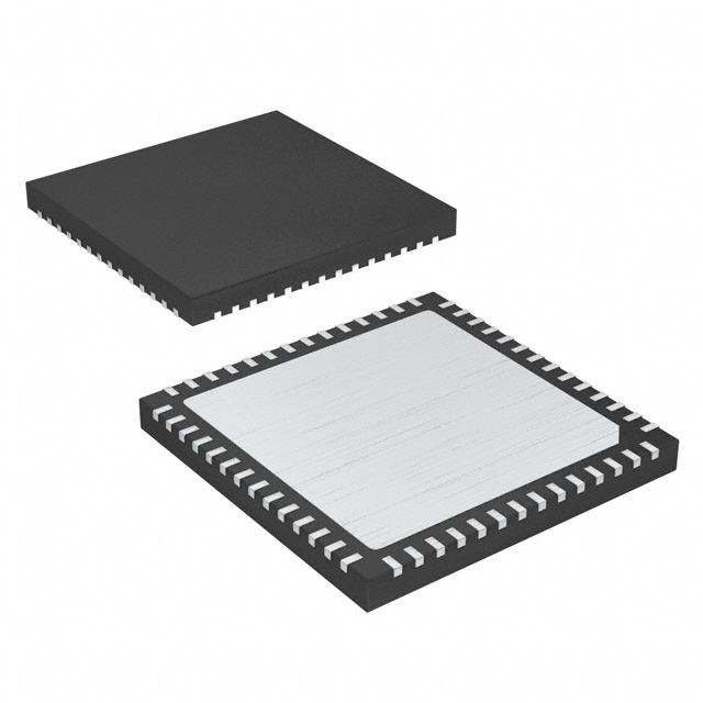
- Part No.:
- MAX16046ETN+CK9
- Manufacturer:
- Analog Devices Inc./Maxim Integrated
- Category:
- Supervisors
- Package:
- 56-WFQFN Exposed Pad
- Datasheet:
-
 MAX16046ETN+CK9.pdf
- Description:
- IC SUPERVISOR 12 CHANNEL 56TQFN
- Quantity:
- Payment:

- Shipping:

Inventory:3,404
Please send an inquiry. Send us your inquiry, and we will respond immediately.
Product details
Overview
MAX16046ETN+CK9 from Maxim Integrated is a 12-channel EEPROM-configurable system manager IC that monitors, sequences, tracks, and margins multiple power supplies in high-reliability systems. It integrates a 1% accurate 10-bit ADC (80–100µs full-cycle time), twelve 8-bit DAC outputs for voltage margining, and twelve configurable sequencing outputs-including four with closed-loop tracking capability-enabling precise control of power-up/down order in server and storage applications.
For engineers reviewing the MAX16046ETN+CK9 datasheet, MAX16046ETN+CK9 pinout, MAX16046ETN+CK9 application, or MAX16046ETN+CK9 equivalent, this device supports dual I²C/SMBus and JTAG configuration interfaces, features nonvolatile fault logging with lock-bit protection, operates across -40°C to +85°C, and delivers ±0.75% ADC total unadjusted error over temperature for robust supply monitoring in mission-critical infrastructure.
Technical Context
The MAX16046ETN+CK9 implements a hierarchical power management architecture: its 10-bit ADC continuously samples up to 12 monitored inputs (MON1–MON12) against independently programmable upper/low/selectable thresholds, triggering fault signals on violation. Each monitored channel supports three selectable input ranges (1.4V, 2.8V, 5.6V), with MON1–MON4 exhibiting 46–100kΩ input impedance and MON5–MON12 at 65–140kΩ.
Its sequencer supports flexible timing via EEPROM-stored delay registers (±5% internal timing accuracy), while four EN_OUT pins (EN_OUT1–EN_OUT4) support closed-loop tracking using external MOSFETs and feedback sense lines (e.g., GPIO1–GPIO4 as INS_ return paths). Six charge-pump-enabled EN_OUT outputs (EN_OUT1–EN_OUT6) drive external MOSFET gates up to VMON_ + 5.6V with 4.5–6µA pull-up current during transitions.
Key Specifications
| Parameter | Value and Actual Design Meaning |
|---|---|
| ADC Resolution | 10-bit with 0.65–0.95%FSR total unadjusted error; enables precise supply voltage detection down to 1.36mV LSB step size (at 1.4V range). |
| DAC Outputs | Twelve 8-bit DACs (DACOUT1–DACOUT12); ±0.8% gain error and ±0.9LSB INL support accurate margining of POL modules within ±1.2mV absolute accuracy at mid-code. |
| Sequencing Channels | 12 independent EN_OUT outputs; EN_OUT1–EN_OUT4 support closed-loop tracking, EN_OUT1–EN_OUT6 support charge-pump gate drive (VMON_ + 5.6V max). |
| Fault Management | Nonvolatile EEPROM fault logger with lock-bit protection; stores failure data persistently after shutdown events for root-cause analysis. |
| Operating Range | VCC = 3V to 14V; specified from -40°C to +85°C; includes 2.7–2.8V DBP regulator and 2.78–2.96V ABP regulator for internal analog/digital domains. |
| Interfaces | I²C/SMBus (400kHz, 0.4V VOL @ 3mA) and JTAG (TCK ≤ 1MHz); both support full EEPROM configuration, register readback, and real-time monitoring. |
| GPIO Flexibility | Six programmable GPIOs (GPIO1–GPIO6); configurable as watchdog I/O (WDI/WDO), manual reset (MR), margin control (MARGINUP/MARGINDN), or dedicated fault outputs. |
Pinout & Package
MAX16046ETN+CK9 is housed in a 56-pin 8mm × 8mm TQFN package with exposed pad (EP), rated for θJA = 21°C/W and θJC = 1°C/W. The package supports reflow soldering at +260°C and lead-free assembly.
| Pin/Terminal | Circuit Role | Design Meaning |
|---|---|---|
| MON1–MON12 | ADC monitored voltage inputs | 12 analog inputs supporting three programmable voltage ranges (1.4V/2.8V/5.6V); MON1–MON4: 46–100kΩ impedance; MON5–MON12: 65–140kΩ impedance. |
| DACOUT1–DACOUT12 | 8-bit DAC output terminals | Twelve voltage outputs for margining DC-DC converters; each configurable for 0.4V/0.6V/0.8V full-scale range with ±0.9LSB integral nonlinearity. |
| EN_OUT1–EN_OUT12 | Configurable sequencing outputs | EN_OUT1–EN_OUT4 support closed-loop tracking; EN_OUT1–EN_OUT6 support charge-pump gate drive (VMON_ + 5.6V); all 12 are EEPROM-configurable as push-pull or open-drain. |
| GPIO1–GPIO6 | Programmable general-purpose I/O | Configurable as WDI/WDO, MR, MARGINUP/MARGINDN, or fault outputs; GPIO1–GPIO4 also serve as return sense lines for tracking loops. |
| SCL/SDA, TCK/TMS/TDI/TDO | Serial configuration interfaces | I²C/SMBus (400kHz) and JTAG (1MHz) enable full EEPROM programming, real-time register access, and fault log readback without requiring external host firmware. |
| DBP/ABP/VCC/GND | Power and bypass terminals | DBP (2.6–2.8V) powers EEPROM/logic; ABP (2.78–2.96V) powers analog circuitry/charge pumps; VCC (3–14V) main supply; EP tied to GND for thermal dissipation. |
Key Features
| Feature | Design Value |
|---|---|
| EEPROM-configurable sequencing | Stores timing delays, power-up/power-down order, and fault response logic in nonvolatile memory-enabling field-upgradable power policies without hardware change. |
| Closed-loop tracking on 4 channels | Uses GPIO-sense return paths and adjustable slew-rate (80–960 V/s) to synchronize ramping of multiple rails within ±150mV differential window during startup/shutdown. |
| Nonvolatile fault event logger | Records first-failure timestamp, fault type, and affected rail in protected EEPROM space; lock bit prevents accidental overwrite during subsequent power cycles. |
| Dual-interface configuration | I²C/SMBus allows integration into existing system management buses; JTAG supports boundary-scan test and factory programming without host software dependency. |
| 12-channel voltage margining | Twelve independent 8-bit DACs inject precise ±1% trim offsets into POL feedback nodes-supporting production-level margin testing per JEDEC JESD22-A108. |
| Flexible GPIO mapping | Six GPIOs support mixed-mode operation: e.g., GPIO2 as MARGINUP, GPIO3 as MARGINDN, GPIO4 as active-low MR, and GPIO5/GPIO6 as WDI/WDO-all set via EEPROM. |
Applications
| Server Power Management | Storage System Sequencing |
|---|---|
|
Use Scenario: Coordinating power sequencing for CPU, memory, and PCIe slots in dual-socket x86 servers with strict ramp-time and hold-time requirements. IC Role / Device Role / Timing Role: Central system manager enforcing inter-rail dependencies (e.g., VCCIO before VDDQ), detecting brownouts via 10-bit ADC, and asserting RESET on fault. Use Value: Eliminates discrete RC timers and comparators; reduces BOM count by integrating 12 ADC channels, 12 DACs, and sequencing logic in one 8mm × 8mm package. |
Use Scenario: Managing power-up sequence of SAS/SATA backplanes, NVMe SSDs, and RAID controllers in enterprise JBOD enclosures. IC Role / Device Role / Timing Role: Configurable EN_OUT outputs drive enable pins of multiple DC-DC converters; closed-loop tracking ensures matched voltage ramps across redundant power domains. Use Value: Prevents back-powering and latch-up during hot-swap events; fault logger captures transient undervoltage events on individual rails for diagnostics. |
| Networking Equipment Monitoring | Workstation Thermal-Aware Control |
|
Use Scenario: Real-time monitoring of 12 supply rails in 10G/25G line cards, including PHY, SerDes, and FPGA core voltages under dynamic load conditions. IC Role / Device Role / Timing Role: ADC scans all MON inputs every 80–100µs; configurable thresholds detect 1% deviations; I²C interface feeds data to host BMC for telemetry and throttling decisions. Use Value: Enables predictive failure analysis via historical voltage trend logging; supports SMBus Alert Response Address (ARA) for interrupt-driven fault reporting. |
Use Scenario: Adaptive voltage margining of GPU and CPU VRMs in high-end workstations during thermal stress testing and overclock validation. IC Role / Device Role / Timing Role: DACOUT outputs apply controlled ±3% voltage offsets to POL trim pins; GPIO2/GPIO3 act as MARGINUP/MARGINDN triggers synchronized with thermal sensor interrupts. Use Value: Replaces manual bench equipment; achieves sub-millivolt margin resolution across temperature (-40°C to +85°C) with ±0.9LSB DAC linearity. |
Equivalent & Alternatives
The following parts are listed as comparable options for similar system management applications.
| Alternative Part | Technical Difference | Application Difference | Selection Advice |
|---|---|---|---|
| MAX16048ETN+ | 8-channel version (vs. 12); identical pinout in 56-pin TQFN but MON9–MON12, DACOUT9–DACOUT12, EN_OUT9–EN_OUT12, and GPIO-related pins are N.C. | Targeted at space-constrained designs with ≤8 rails; lacks closed-loop tracking on MON9–MON12 and reduced margining capacity. | Select MAX16048ETN+ only when system has ≤8 monitored supplies and board layout must reuse MAX16046 footprint without redesign. |
| TPS40400RHLR | 6-channel PMBus-compliant controller; no integrated ADC/DAC; relies on external resistive dividers and digital margining via PMBus WRITE_VOUT_COMMAND. | Requires host processor for sequencing logic; no nonvolatile fault logging; supports only 6 rails and no closed-loop tracking. | Choose TPS40400RHLR for PMBus-centric architectures where centralized firmware manages policy, not distributed autonomous sequencing. |
Compared with MAX16048ETN+, MAX16046ETN+CK9 provides 50% more monitoring/margining channels and full closed-loop tracking capability-critical for complex multi-rail servers. Versus TPS40400RHLR, it eliminates host dependency with autonomous EEPROM-based sequencing and integrated analog sensing, reducing system-level latency and firmware overhead.
Availability
MAX16046ETN+CK9 is available at Aetrix Electronics and suitable for servers, storage systems, networking equipment, and workstations requiring stable component supply, long-term lifecycle support, and guaranteed traceable sourcing for industrial and datacenter deployments.
Supply support for MAX16046ETN+CK9 includes scheduled delivery planning, volume procurement assistance, BOM continuity management, traceable sourcing, and lifecycle availability coordination for OEM customers, industrial embedded developers, connected-device designers, and electronics production programs.
Manufacturer
Maxim Integrated, now part of Analog Devices, designs precision analog, mixed-signal, and power management ICs for demanding industrial, communications, and computing applications.
The MAX16046ETN+CK9 belongs to Maxim's EEPROM-programmable system manager product line, engineered specifically for autonomous, fault-resilient power sequencing and monitoring in high-availability infrastructure where deterministic behavior and nonvolatile event logging are mandatory.
FAQ
What is the primary function of the MAX16046ETN+CK9 in a server power architecture?
The MAX16046ETN+CK9 serves as the central autonomous power manager in server motherboards, performing real-time monitoring of up to 12 voltage rails via its 10-bit ADC, executing EEPROM-defined power-up/down sequences across 12 EN_OUT outputs, applying precise voltage margining through twelve 8-bit DACs, and logging faults to nonvolatile memory. Its closed-loop tracking capability on four channels ensures synchronized ramping of critical rails like CPU VDD and memory VDDQ, directly preventing latch-up and ensuring compliance with Intel VRD and AMD SVI2 specifications.
How does the MAX16046ETN+CK9 handle fault events and ensure diagnostic traceability?
The MAX16046ETN+CK9 includes a dedicated nonvolatile fault logger that records the first occurrence of any detected fault-including overvoltage, undervoltage, or tracking violation-into internal EEPROM. Upon fault assertion, it sets a lock bit to prevent accidental erasure during subsequent power cycles. Engineers can retrieve timestamped fault data, affected rail identifier, and threshold violation magnitude via I²C or JTAG, enabling root-cause analysis without requiring continuous host polling or external logging hardware.
Can the MAX16046ETN+CK9 be configured without host processor intervention?
Yes, the MAX16046ETN+CK9 supports fully autonomous operation after initial configuration. Its EEPROM stores all sequencing delays, voltage thresholds, DAC settings, GPIO modes, and fault response policies. Once programmed via I²C or JTAG, it executes power policies independently-no host firmware, driver, or runtime supervision is required. This makes it ideal for headless systems, secure boot environments, or designs where host processor initialization may lag behind power rail availability.
What are the key electrical differences between the MAX16046ETN+CK9 and MAX16048ETN+?
The MAX16046ETN+CK9 supports 12 monitored inputs (MON1–MON12), 12 DAC outputs (DACOUT1–DACOUT12), and 12 sequencing outputs (EN_OUT1–EN_OUT12), while the MAX16048ETN+ supports only 8 of each. In the 56-pin TQFN package, pins assigned to MON9–MON12, DACOUT9–DACOUT12, and EN_OUT9–EN_OUT12 are No Connect on MAX16048ETN+. Both share identical ADC accuracy (±0.75%FSR), DAC linearity (±0.9LSB INL), and operating temperature range (-40°C to +85°C).
Does the MAX16046ETN+CK9 support both I²C and JTAG interfaces simultaneously?
Yes, the MAX16046ETN+CK9 supports concurrent use of I²C/SMBus and JTAG interfaces. SCL/SDA and TCK/TMS/TDI/TDO operate independently-allowing I²C to handle runtime monitoring and fault reporting while JTAG is used for factory programming, boundary-scan testing, or debug access without disrupting system operation. Both interfaces provide full read/write access to all configuration registers, ADC results, DAC values, and fault log contents.
MAX16046ETN+CK9 Specifications
- Product attributes
- Attribute value
- Manufacturer:
- Analog Devices Inc./Maxim Integrated
- Series:
- -
- Package/Case:
- 56-WFQFN Exposed Pad
- Packaging:
- Tube
- Product Status:
- Obsolete
- Programmable:
- Not Verified
- Type:
- System Manager
- Number of Voltages Monitored:
- 12
- Voltage - Threshold:
- Adjustable/Selectable
- Output:
- Open Drain, Push-Pull
- Reset:
- Active Low
- Reset Timeout:
- Adjustable/Selectable
- Operating Temperature:
- -40°C ~ 85°C (TA)
- Grade:
- -
- Qualification:
- -
- Mounting Type:
- Surface Mount
- Supplier Device Package:
- 56-TQFN (8x8)
MAX16046ETN+CK9 FAQ
1.How can I place an order for MAX16046ETN+CK9 through Aetrix?
Please submit a Request for Quotation (RFQ) for MAX16046ETN+CK9 on Aetrix. Our sales agent will provide a competitive quotation and guide you through the order confirmation once you accept the terms.
2.Are the price and stock information for MAX16046ETN+CK9 reliable?
The price and inventory of MAX16046ETN+CK9 are updated periodically and may fluctuate due to market conditions. Stock and pricing data are typically refreshed every 24 hours. Quotation validity for MAX16046ETN+CK9 is usually 5 days.
3.What payment methods are accepted for MAX16046ETN+CK9?
We accept Wire Transfer, PayPal, Credit Card, Western Union, MoneyGram, and Escrow for MAX16046ETN+CK9 transactions.
Note: Certain payment methods may incur a processing fee.
4.How is shipping managed for MAX16046ETN+CK9?
MAX16046ETN+CK9 orders can be shipped via leading logistics carriers, including DHL, UPS, FedEx, TNT, or Registered Mail.
Once your MAX16046ETN+CK9 order is processed, you will receive an email with the shipment details and tracking number.
Note: Tracking information may take up to 24 hours to appear. Express delivery typically takes 3–5 business days.
5.How can I obtain technical support or documentation for MAX16046ETN+CK9?
For technical support, including MAX16046ETN+CK9 datasheets, pinout diagrams, or application guidance, please contact our engineering support team. They can provide detailed documentation and assistance for your MAX16046ETN+CK9 requirements.
6.How does Aetrix verify that MAX16046ETN+CK9 is sourced from the original manufacturer or authorized distributors?
All MAX16046ETN+CK9 products on Aetrix are procured from qualified distributors and authorized channels. Our dedicated quality assurance team conducts strict verification, including traceability checks and, if necessary, third-party testing. This ensures that MAX16046ETN+CK9 meets industry standards.
7.What is the process for return or replacement of MAX16046ETN+CK9?
All MAX16046ETN+CK9 units undergo pre-shipment inspection (PSI). If there is an issue with MAX16046ETN+CK9, returns or replacements are accepted under the following conditions:
1.Quantity discrepancies, incorrect items, or visible external defects (such as breakage or corrosion), acknowledged by Aetrix.
2.The issue is reported within 90 days of delivery.
3.The MAX16046ETN+CK9 part is unused and in its original packaging.
Return procedure for MAX16046ETN+CK9:
1.Submit a request within 90 days.
2.Obtain a Return Material Authorization (RMA) from Aetrix.
MAX16046ETN+CK9 Tags
-
MIC826SYMT-TR
Microchip Technology

-
APX803S-31SA-7
Diodes Incorporated
-
APX803L20-29SA-7
Diodes Incorporated

-
TPS3828-33DBVR
Texas Instruments

-
V6340RSP3B+
EM Microelectronic
-
EM6325CXSP5B-2.9+
EM Microelectronic
-
MCP120T-300I/TT
Microchip Technology
-
MCP130T-315I/TT
Microchip Technology
-
MCP120T-475I/TT
Microchip Technology
-
MCP111T-300E/TT
Microchip Technology
-
MCP120T-315I/TT
Microchip Technology
-
MCP809T-315I/TT
Microchip Technology
Tech Hub

A practical engineering guide to 3.3V and 5V logic compatibility, input thresholds, resistor dividers, translator ICs, MOSFET level shifting, I2C pull-ups, timing limits and power-sequencing risks.

The 74HC595 uses push-pull logic outputs, while the TPIC6B595 uses 50 V open-drain DMOS sinks for higher-power loads. This guide compares timing, current limits, 3.3 V interfacing, load wiring, thermal…

The 74HC595 converts serial data into eight stable parallel outputs. This guide covers pin functions, shift and storage timing, OE and MR behavior, drive-current limits, cascading, voltage compatibilit…

A technical comparison of level-sensitive latches and edge-triggered flip-flops, covering timing windows, setup and hold limits, master–slave operation, time borrowing, race-through, HDL inference and…

A D latch stores one bit while Enable controls when data can pass. This reference covers gate-level operation, truth tables, transparency, setup and hold timing, LE versus OE, common ICs and practical …

An SR latch stores one bit through cross-coupled feedback. This engineering reference covers NOR and NAND implementations, truth tables, forbidden-state recovery, gated operation, switch debouncing, fa…

Latch circuits retain one bit through feedback. This technical reference covers SR and D latches, truth tables, transparency, timing limits, latch-versus-flip-flop behavior, applications and common log…

An engineering guide to LED driver operation, constant-current and constant-voltage outputs, linear and switching topologies, dimming, IC selection, calculations, replacement compatibility, and fault c…

Operational amplifier guide covering op amp basics, feedback, ideal vs real op amps, common configurations, buffer circuits, offset, bias current, gain-bandwidth, slew rate, rail-to-rail limits and sel…

Jumper cables guide covering safe connection order, red and black clamp placement, final ground connection, cable gauge, length, clamp quality, copper vs CCA cables, jump starter comparison and battery…


