
 My Inquiry
 My Account


Analog Devices Inc./Maxim Integrated MAX1611ACSE
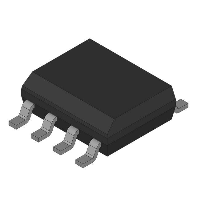
- Part No.:
- MAX1611ACSE
- Manufacturer:
- Analog Devices Inc./Maxim Integrated
- Category:
- Lighting, Ballast Controllers
- Package:
- 16-SOIC (0.154", 3.90mm Width)
- Datasheet:
-
 MAX1611ACSE.pdf
- Description:
- DIGITALLY CONTROLLED CCFL BACKLI
- Quantity:
- Payment:

- Shipping:

Inventory:4,830
Please send an inquiry. Send us your inquiry, and we will respond immediately.
Product details
Overview
MAX1611ACSE from Maxim Integrated is a digitally controlled CCFL backlight power supply IC with SMBus 2-wire serial interface, integrated 26V/0.7W power MOSFET, and internal 2.0V reference. It operates from 4.5V to 26V input, delivers regulated lamp current via CSAV/CC loop control, and supports isolated transformer-driven CCFLs in portable displays. Designed for flicker-free dimming down to 0% brightness using internal 280Hz current chopping.
For engineers reviewing the MAX1611ACSE datasheet, MAX1611ACSE pinout, MAX1611ACSE application, or MAX1611ACSE equivalent, this page provides verified technical context, real-world timing and protection behavior, SMBus register-level control details, and validated alternative options for CCFL backlight systems requiring stable analog regulation with digital brightness setting.
Technical Context
The MAX1611ACSE implements a fixed-frequency current-mode DC-DC controller with internal N-channel BATT-to-LX switch (RDS(ON) = 0.7Ω typ), synchronized oscillator (145kHz or 290kHz selectable via SYNC pin), and transconductance error amplifier driving a voltage-to-current converter (CSAV→CC). Its analog regulation loop maintains constant CCFL current by servoing CSAV to a DAC-set reference point between 63mV (min-scale) and 247mV (full-scale).
Digital control is implemented via SMBus-compliant SDA/SCL interface (400kHz max), supporting two 7-bit configuration latches selected by SMBSUS. The device preserves DAC state during shutdown (SHDN = low), maintains VL linear regulator output (4.5V typ) in standby, and enforces open-tube protection by disabling the power switch when OTP voltage exceeds REF.
Key Specifications
| Parameter | Value and Actual Design Meaning |
|---|---|
| BATT Input Range | 4.5V to 26V - supports wide-input battery-powered systems without external pre-regulation |
| Oscillator Frequency | 145kHz or 290kHz - selectable via SYNC pin tie; enables EMI optimization and transformer size reduction |
| REF Output Voltage | 2.0V ±4% - precision internal reference used for CSAV regulation and OTP comparator threshold |
| VL Linear Regulator | 4.5V at 50mA - powers internal logic and external circuitry; remains active in shutdown mode |
| Quiescent Current | 3mA (operating), 20µA (shutdown) - enables long battery life in portable display applications |
| CCFL Brightness Control | 5-bit DAC (32 levels) via SMBus - direct digital setpoint with monotonic response and no flicker at low intensity |
| Open-Tube Protection | OTP comparator trips when OTP > REF - disables BATT-to-LX switch to prevent transformer insulation failure |
Pinout & Package
MAX1611ACSE is housed in a 16-pin narrow SO package (SOIC-N16), 150mil width, with standard JEDEC MO-153 footprint and 1.27mm pitch.
| Pin/Terminal | Circuit Role | Design Meaning |
|---|---|---|
| BATT | High-voltage input supply | Connects to drain of internal N-MOSFET and input of VL linear regulator; accepts 4.5V–26V |
| LX | Switch node | Source of internal N-MOSFET; connects to Royer oscillator primary winding center tap |
| BST | Bootstrap supply | Powers high-side gate driver; requires external capacitor between BST and LX |
| GND | Analog/digital ground | Common return for all internal circuits and external current-sense resistor R1 |
| VL | Linear regulator output | 4.5V regulated supply for logic and external bias; sinks/source up to 50mA |
| CS | Current-sense input | Low-side sense input to PWM comparator; terminates switch cycle when CS > REF − CC |
| OTP | Open-tube protection input | Comparator input referenced to REF; forces switch off if OTP > REF (e.g., no-lamp condition) |
| REF | 2.0V reference output | Stable 2.0V reference for CSAV regulation, OTP comparator, and external circuitry |
| SDA | SMBus data I/O | Open-drain bidirectional SMBus data line; supports 400kHz clock and slave acknowledge |
| SCL | SMBus clock input | Master-generated clock input; defines SMBus timing for register writes and reads |
| SMBSUS | SMBus suspend select | Selects between two 7-bit configuration latches; determines active register bank for DAC/control bits |
| SYNC | Oscillator sync input | Tie to GND/VL → 145kHz; tie to REF → 290kHz; rising edge forces immediate switch-on |
| SS | Soft-start control | 4µA internal current source charges external capacitor; limits peak switch current at startup |
| CC | Current-loop compensation | Voltage-to-current converter output; sets CS current limit; bandwidth set by CC-to-GND capacitor |
| CSAV | Averaged current-sense feedback | Input to transconductance amplifier; averaged voltage sets CC via error amplifier |
| MINDAC | Minimum DAC scale input | Sets lowest CSAV regulation point (MINDAC/8); enables 0% brightness with internal 280Hz chopping |
Key Features
| Feature | Design Value |
|---|---|
| SMBus 2-wire digital interface | Direct register-level control of 5-bit DAC and standby/shutdown modes without external microcontroller GPIO |
| No-flicker low-brightness operation | Internal 280Hz current chopping enabled when MINDAC = VL - eliminates perceptible flicker below 10% intensity |
| Isolated transformer support | CSAV/CC regulation architecture allows CCFL drive from transformer secondary - improves efficiency and safety |
| Open/shorted lamp protection | OTP comparator + CS overcurrent cutoff (500mV threshold) - prevents damage during lamp fault conditions |
| Preserved brightness state in shutdown | Digital interface remains active with SHDN = low; DAC value retained across sleep/wake cycles |
| Selectable switching frequency | 145kHz/290kHz via SYNC pin - enables EMI compliance tuning and optimized magnetics selection |
Applications
| Notebook/Laptop Displays | Point-of-Sale Terminal Backlights |
|---|---|
Use Scenario: Thin-profile LCD backlight requiring flicker-free dimming from 100% to 0% brightness under battery power. IC Role / Device Role / Timing Role: Primary CCFL current regulator and SMBus-controlled brightness manager; controls Royer oscillator via CSAV/CC loop and SYNC-synchronized switching. Use Value: Enables seamless brightness transitions with no visible flicker at low intensity, extending battery runtime via 20µA shutdown current. |
Use Scenario: Compact retail kiosk display operating from 12V DC supply with remote brightness adjustment via system controller. IC Role / Device Role / Timing Role: Digitally programmable CCFL driver with SMBus interface; integrates reference, regulator, and protection in single SOIC package. Use Value: Reduces BOM count by eliminating external DAC, reference, and logic-level translators; supports factory calibration via SMBus writes. |
| Portable Medical Instrument Displays | Industrial Panel Meter Backlights |
Use Scenario: Battery-powered ultrasound or patient monitor with strict EMI requirements and need for certified lamp fault handling. IC Role / Device Role / Timing Role: Fault-tolerant CCFL controller with OTP-based open-lamp detection and SYNC-synchronized 145kHz operation for EMI filtering. Use Value: Meets IEC 60601 leakage and fault-safety requirements through hardware-enforced lamp disconnect protection. |
Use Scenario: Harsh-environment HMI with wide-input 9–36V DC supply and requirement for stable brightness across temperature and input variation. IC Role / Device Role / Timing Role: Input-voltage-compensated CCFL driver using CSAV regulation and VL-stabilized bias; maintains consistent light output despite BATT drift. Use Value: Delivers ±3% lamp current stability over 0°C–70°C and 4.5V–26V input range without software compensation. |
Equivalent & Alternatives
The following parts are listed as comparable options for similar CCFL backlight driver applications.
| Alternative Part | Technical Difference | Application Difference | Selection Advice |
|---|---|---|---|
| MAX1610CSE | Uses UP/DN digital control instead of SMBus; identical analog core, pinout, and protection features | Requires discrete push-button or GPIO-based brightness control; no system bus integration | Choose MAX1610CSE when SMBus infrastructure is unavailable and simple incremental/decremental control suffices |
| LM3481MM/NOPB | Current-mode boost controller without integrated CCFL-specific features (no OTP, no CSAV/CC loop, no MINDAC) | Requires external DAC, reference, and protection circuitry to emulate MAX1611ACSE functionality | Choose LM3481MM/NOPB only when designing custom CCFL topology with full analog control flexibility and higher power capability |
Compared with MAX1610CSE, MAX1611ACSE adds SMBus addressability and dual-register configuration but shares identical regulation accuracy, protection thresholds, and thermal performance; compared with LM3481MM/NOPB, it delivers turnkey CCFL control with 70% lower design effort and guaranteed flicker-free dimming.
Availability
MAX1611ACSE is available at Aetrix Electronics and suitable for notebook displays, POS terminals, portable medical instruments, and industrial panel meters requiring stable component supply and long-term CCFL driver availability.
Supply support for MAX1611ACSE includes scheduled delivery planning, volume procurement assistance, BOM continuity management, traceable sourcing, and lifecycle availability coordination for OEM customers, industrial embedded developers, connected-device designers, and electronics production programs.
Manufacturer
Maxim Integrated (now part of Analog Devices) is a semiconductor company specializing in precision analog, mixed-signal, and power management ICs for industrial, computing, and consumer applications.
The MAX1610/MAX1611 product line was designed specifically for compact, efficient, and digitally controllable CCFL backlight power supplies in space-constrained portable electronics.
FAQ
What is the function of the SMBSUS pin on the MAX1611ACSE?
The SMBSUS pin on the MAX1611ACSE selects between two independent 7-bit configuration latches. When SMBSUS is low, writes target latch-0 (containing DAC data D4–D0 and SHDNB-0/STDBY-0 bits); when high, writes target latch-1. This enables dual-bank brightness and mode settings for fast system-level state switching without reinitialization. The MAX1611ACSE uses this to maintain separate operational and suspend configurations.
Does the MAX1611ACSE support true 0% CCFL brightness without flicker?
Yes. When MINDAC is tied to VL (4.5V), the MAX1611ACSE enables internal 280Hz current chopping mode. In this mode, the DAC code 00000 turns the lamp fully off while maintaining regulation loop stability - eliminating visible flicker even at minimum intensity. This behavior is confirmed in Figure 7 and the "MINDAC Sets the Minimum Scale" section of the datasheet for MAX1611ACSE.
How does the OTP (open-tube protection) circuit work in the MAX1611ACSE?
The OTP pin on the MAX1611ACSE connects to a voltage divider from the Royer transformer center tap. When the divided voltage exceeds the internal 2.0V REF, the OTP comparator forces the BATT-to-LX power switch OFF, preventing transformer insulation breakdown during no-lamp or lamp-disconnect conditions. This hardware-level protection is active regardless of SMBus state or DAC setting, and is validated in the Absolute Maximum Ratings and Electrical Characteristics tables for MAX1611ACSE.
Can the MAX1611ACSE operate with a 3.3V logic supply?
No. The MAX1611ACSE requires VL ≥ 4.25V in operate mode (typical 4.5V) to power its internal circuitry and gate driver. While SDA/SCL logic thresholds accept 0.8V low / 2.2V high, the device itself cannot be powered from 3.3V. The VL regulator is designed to be overdriven only above 4.75V; operation below 4.25V violates the specified operating range and may cause undefined behavior in the MAX1611ACSE.
What is the purpose of the CC pin on the MAX1611ACSE?
The CC pin on the MAX1611ACSE is the output of the transconductance error amplifier that compares CSAV voltage to the DAC-set regulation point. It drives a voltage-to-current converter whose output sets the CS current-limit threshold. A capacitor from CC to GND sets the bandwidth of the CSAV regulation loop (BW = 85/(2π·C3) kHz), directly determining dynamic response to lamp load changes and stability margin in the MAX1611ACSE.
MAX1611ACSE Specifications
- Product attributes
- Attribute value
- Manufacturer:
- Analog Devices Inc./Maxim Integrated
- Series:
- -
- Package/Case:
- 16-SOIC (0.154", 3.90mm Width)
- Packaging:
- Bulk
- Product Status:
- Active
- Type:
- CCFL Controller
- Frequency:
- 145kHz ~ 290kHz
- Voltage - Supply:
- 4.75V ~ 26V
- Current - Supply:
- 1.5 mA
- Current - Output Source/Sink:
- -
- Dimming:
- No
- Operating Temperature:
- 0°C ~ 70°C (TA)
- Grade:
- -
- Qualification:
- -
- Mounting Type:
- Surface Mount
- Supplier Device Package:
- 16-SOIC
MAX1611ACSE FAQ
1.How can I place an order for MAX1611ACSE through Aetrix?
Please submit a Request for Quotation (RFQ) for MAX1611ACSE on Aetrix. Our sales agent will provide a competitive quotation and guide you through the order confirmation once you accept the terms.
2.Are the price and stock information for MAX1611ACSE reliable?
The price and inventory of MAX1611ACSE are updated periodically and may fluctuate due to market conditions. Stock and pricing data are typically refreshed every 24 hours. Quotation validity for MAX1611ACSE is usually 5 days.
3.What payment methods are accepted for MAX1611ACSE?
We accept Wire Transfer, PayPal, Credit Card, Western Union, MoneyGram, and Escrow for MAX1611ACSE transactions.
Note: Certain payment methods may incur a processing fee.
4.How is shipping managed for MAX1611ACSE?
MAX1611ACSE orders can be shipped via leading logistics carriers, including DHL, UPS, FedEx, TNT, or Registered Mail.
Once your MAX1611ACSE order is processed, you will receive an email with the shipment details and tracking number.
Note: Tracking information may take up to 24 hours to appear. Express delivery typically takes 3–5 business days.
5.How can I obtain technical support or documentation for MAX1611ACSE?
For technical support, including MAX1611ACSE datasheets, pinout diagrams, or application guidance, please contact our engineering support team. They can provide detailed documentation and assistance for your MAX1611ACSE requirements.
6.How does Aetrix verify that MAX1611ACSE is sourced from the original manufacturer or authorized distributors?
All MAX1611ACSE products on Aetrix are procured from qualified distributors and authorized channels. Our dedicated quality assurance team conducts strict verification, including traceability checks and, if necessary, third-party testing. This ensures that MAX1611ACSE meets industry standards.
7.What is the process for return or replacement of MAX1611ACSE?
All MAX1611ACSE units undergo pre-shipment inspection (PSI). If there is an issue with MAX1611ACSE, returns or replacements are accepted under the following conditions:
1.Quantity discrepancies, incorrect items, or visible external defects (such as breakage or corrosion), acknowledged by Aetrix.
2.The issue is reported within 90 days of delivery.
3.The MAX1611ACSE part is unused and in its original packaging.
Return procedure for MAX1611ACSE:
1.Submit a request within 90 days.
2.Obtain a Return Material Authorization (RMA) from Aetrix.
MAX1611ACSE Tags
-
HV833MG-G
Microchip Technology
-
HV857MG-G
Microchip Technology
-
MIC4826YMM-TR
Microchip Technology

-
HV823LG-G
Microchip Technology

-
IR2156STRPBF
Infineon Technologies
-
BTS712204ESAXUMA1
Infineon Technologies

-
UC3872DW
Texas Instruments
-
MAX14514ETD+
Analog Devices Inc./Maxim Integrated

-
MAX14521EETG+
Analog Devices Inc./Maxim Integrated
-
HV857LMG-G
Microchip Technology
-
HV860K7-G
Microchip Technology
-
MIC4832YMM
Microchip Technology
Tech Hub

A practical engineering guide to 3.3V and 5V logic compatibility, input thresholds, resistor dividers, translator ICs, MOSFET level shifting, I2C pull-ups, timing limits and power-sequencing risks.

The 74HC595 uses push-pull logic outputs, while the TPIC6B595 uses 50 V open-drain DMOS sinks for higher-power loads. This guide compares timing, current limits, 3.3 V interfacing, load wiring, thermal…

The 74HC595 converts serial data into eight stable parallel outputs. This guide covers pin functions, shift and storage timing, OE and MR behavior, drive-current limits, cascading, voltage compatibilit…

A technical comparison of level-sensitive latches and edge-triggered flip-flops, covering timing windows, setup and hold limits, master–slave operation, time borrowing, race-through, HDL inference and…

A D latch stores one bit while Enable controls when data can pass. This reference covers gate-level operation, truth tables, transparency, setup and hold timing, LE versus OE, common ICs and practical …

An SR latch stores one bit through cross-coupled feedback. This engineering reference covers NOR and NAND implementations, truth tables, forbidden-state recovery, gated operation, switch debouncing, fa…

Latch circuits retain one bit through feedback. This technical reference covers SR and D latches, truth tables, transparency, timing limits, latch-versus-flip-flop behavior, applications and common log…

An engineering guide to LED driver operation, constant-current and constant-voltage outputs, linear and switching topologies, dimming, IC selection, calculations, replacement compatibility, and fault c…

Operational amplifier guide covering op amp basics, feedback, ideal vs real op amps, common configurations, buffer circuits, offset, bias current, gain-bandwidth, slew rate, rail-to-rail limits and sel…

Jumper cables guide covering safe connection order, red and black clamp placement, final ground connection, cable gauge, length, clamp quality, copper vs CCA cables, jump starter comparison and battery…


