
 My Inquiry
 My Account


Analog Devices Inc./Maxim Integrated MAX20095ATIA/VY+
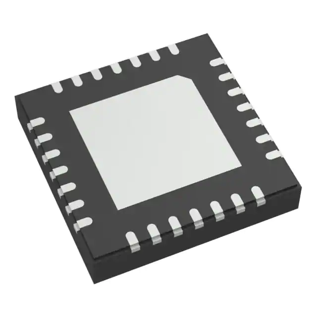
- Part No.:
- MAX20095ATIA/VY+
- Manufacturer:
- Analog Devices Inc./Maxim Integrated
- Category:
- Battery Management
- Package:
- 28-WFQFN Exposed Pad
- Datasheet:
-
 MAX20095ATIA/VY+.pdf
- Description:
- IC BAT MFUNC MULT-CHEM 1C 28TQFN
- Quantity:
- Payment:

- Shipping:

Inventory:3,301
Please send an inquiry. Send us your inquiry, and we will respond immediately.
Product details
Overview
The MAX20095ATIA/VY+ from Analog Devices is a highly integrated automotive-grade backup battery charger and synchronous boost controller IC. It delivers configurable constant-current/constant-voltage (CC/CV) charging up to 1A, supports lithium or NiMH backup batteries, provides precision battery state-of-health (SOH) diagnostics via internal current sink (0–2A), and generates regulated 5V–12V boost output up to 3.5A during primary power loss - enabling uninterrupted operation of telematics and safety-critical ECUs.
For engineers reviewing the MAX20095ATIA/VY+ datasheet, MAX20095ATIA/VY+ pinout, MAX20095ATIA/VY+ application, or MAX20095ATIA/VY+ equivalent, this page details its dual-function architecture, I²C-configurable thresholds (CV voltage, CC current, boost OV/UV), 2.2MHz switching frequency for compact magnetics, AEC-Q100 qualification, and side-wettable TQFN-28 package for automated optical inspection in automotive production.
Technical Context
The MAX20095ATIA/VY+ integrates two independent but interlocked functional blocks: a programmable CC/CV battery charger (3.0–6.0V CV, 50mA–1A CC) with EN1B hardware disable and thermal foldback, and a high-efficiency synchronous boost controller with factory-set output (5.4V–12.3V range), 2.2MHz PWM/PFM operation, and automatic wake/sleep based on SUP2 voltage relative to BOOST_OV_F (104–110.5%) and BOOST_UVLO (65–85%).
Its diagnostic subsystem includes an I²C-accessible 0–2A precision current sink (±10% accuracy at 0.5A) with analog readout via AVI and AVB pins, remote BUB voltage sensing (BATTS), and open-drain status outputs (STATUSB, BUBTRIG) synchronized to boost activation. All logic is governed by a deterministic state machine with explicit enable/disable conditions per block to prevent concurrent operation.
Key Specifications
| Parameter | Value and Actual Design Meaning |
|---|---|
| Input Voltage Range (SUP2) | 3.5V to 36V - supports wide automotive battery rail; 40V load-dump tolerant for robustness. |
| Boost Output Voltage | Factory-programmable 5.4V–12.3V - enables direct compatibility with 5V, 8V, 9V, or 12V system rails without external feedback dividers. |
| Charging Current Range | 50mA to 1A (I²C-settable) - covers precharge, fast-charge, and maintenance modes for single/multicell Li-ion or NiMH. |
| SOH Current Sink Range | 0A to 2A (I²C-controlled) - enables accurate impedance measurement and capacity estimation of backup batteries under real operating conditions. |
| Switching Frequency | 1.9MHz to 2.3MHz (typ 2.2MHz) - allows use of small 1µH–2.2µH inductors, reducing solution size and cost. |
| Operating Temperature | −40°C to +125°C - qualified per AEC-Q100 Grade 0, suitable for under-hood and infotainment module deployment. |
| Package | 28-pin side-wettable TQFN (5mm × 5mm × 0.75mm) - enables automated optical inspection (AOI) of solder joints for zero-defect automotive manufacturing. |
Pinout & Package
MAX20095ATIA/VY+ uses a 28-pin, 5mm × 5mm side-wettable TQFN package (package code T2855Y+5C) with exposed pad for thermal dissipation. θJA = 35°C/W on 4-layer board.
| Pin/Terminal | Circuit Role | Design Meaning |
|---|---|---|
| SUP1 | CC/CV Charger Input | Accepts 0–6.5V input; powers charger block; requires local 2.2µF ceramic decoupling. |
| BATTP | Charger Output / SOH Current Sink Anode | Delivers charge current to backup battery; serves as current sink terminal during SOH measurements. |
| SNK | SOH External MOSFET Source Connection | Connects to source of external N-channel MOSFET (M4) used to discharge BUB during impedance testing. |
| G2 | SOH MOSFET Gate Driver | Drives gate of M4 for 62µs before SOH current ramp; controlled exclusively via I²C. |
| AVI | Analog Readout of SOH Sink Current | Provides voltage proportional to ISNK (gain = 440 A/A); used with IMON resistor to monitor discharge current. |
| AVB | Analog Battery Voltage Sense Output | Routes filtered BUB voltage to external ADC; includes 10µs-delayed 60kΩ pull-down for stable sampling. |
| STATUSB | Open-Drain Boost Active Indicator | Active-low signal pulled to AGND when boost is regulating SUP2 - enables shared interrupt handling with microcontroller. |
| BUBTRIG | Backup Activation Pulse Output | Drives BIAS for 180–220ms upon boost start - provides timed trigger for host system to initiate failover procedures. |
| EN1B | Hardware Charger Disable | Active-high pin that forces immediate charger shutdown and state-machine reset - used for system-level fault response. |
| VDDIO | I²C Logic Supply | Accepts 2.5V–5.5V; powers SDA/SCL interface; must match host bus voltage for reliable communication. |
| SCL/SDA | I²C Configuration & Status Interface | Supports standard-mode (400kHz) operation; enables full register access for configuration, monitoring, and diagnostics. |
| SUP2 | System Supply Input / Boost Output Node | High-voltage input (3.5–36V); also serves as regulated boost output (5.4–12.3V) during primary power loss. |
| DL/DH/LX/BST | Boost Power Stage Control & Switching Nodes | Drive external N-channel MOSFETs; LX is switching node; BST supplies high-side gate drive; DL/DH are complementary drivers. |
| CSP/CSN | Current-Sense Inputs | Differential inputs for boost inductor current sensing; require Kelvin connection to sense resistor for ±10% accuracy. |
| COMP | Loop Compensation Node | Output of internal transconductance amplifier; connects to RC network for stability tuning per application requirements. |
Key Features
| Feature | Design Value |
|---|---|
| Configurable CC/CV Charging | I²C-selectable CV voltage (3.0–6.0V) and CC current (50mA–1A) - supports diverse battery chemistries and cell counts without hardware change. |
| Integrated SOH Diagnostics | Precision 0–2A current sink with ±10% accuracy and analog readout (AVI/AVB) - enables field-deployable battery health assessment without external instrumentation. |
| Automotive-Grade Robustness | AEC-Q100 Grade 0 qualification, 40V load-dump tolerance, <1µA leakage on battery-connected pins, and −40°C to +125°C operation - meets ASIL-B system requirements. |
| Low-Leakage Backup Path | <1µA BATTP and BATTS leakage current - preserves backup battery charge over extended vehicle off-time (e.g., parking mode). |
| Optimized for Small Form Factor | 2.2MHz switching frequency and integrated gate drivers - eliminate need for external boost drivers and reduce inductor size by >50% vs. 500kHz solutions. |
Applications
| Automotive Telematics Backup | ADAS Event Recorder Power |
|---|---|
|
Use Scenario: Maintains LTE/GNSS connectivity and data upload during engine-off periods in connected car platforms. IC Role / Device Role / Timing Role: Dual-role IC providing continuous CC/CV charging of supercapacitor or Li-ion backup while delivering regulated 5V/12V boost output upon ignition loss. Use Value: Enables >72-hour telematics uptime with <1µA quiescent drain; eliminates need for separate charger + boost IC, saving 32mm² PCB area. |
Use Scenario: Powers camera buffer memory and secure logging circuitry during collision-triggered recording in lane-departure or AEB systems. IC Role / Device Role / Timing Role: Acts as failover power manager - monitors main battery, initiates boost within 200ms (BUBTRIG pulse), and sustains 3.5A peak load for ≥5s. Use Value: Guarantees uninterrupted video capture during critical events; thermal-limit protection (145°C) prevents shutdown during sustained burst recording. |
| Infotainment Head Unit Retention | Body Control Module (BCM) Keep-Alive |
|
Use Scenario: Preserves radio presets, navigation history, and Bluetooth pairing across vehicle sleep/wake cycles in premium audio head units. IC Role / Device Role / Timing Role: Provides low-noise 5V bias to MCU and RAM retention circuits; uses AGND/PGND separation and remote BATTS sensing for ±0.5% voltage regulation. Use Value: Eliminates capacitor-based hold-up limitations; extends retention time from seconds to weeks using small 100mAh Li-ion cell. |
Use Scenario: Maintains CAN communication, door lock status, and intrusion detection logic during vehicle park mode with <100µA total system draw. IC Role / Device Role / Timing Role: Delivers ultra-low-IQ standby (26µA typical) and seamless switchover to backup battery - no brownout or reset during transition. Use Value: Reduces BCM standby current by 60% vs. discrete solutions; side-wettable TQFN ensures AOI-compatible solder joint reliability for 15-year automotive life. |
Equivalent & Alternatives
The following parts are listed as comparable options for similar backup battery management applications.
| Alternative Part | Technical Difference | Application Difference | Selection Advice |
|---|---|---|---|
| MAX20094ATIA/VY+ | Identical pinout and feature set, but factory-programmed for fixed 6.2V boost output (vs. MAX20095's 12V option); same SOH and charger specs. | Best suited for 5V/6V system rails where programmability is unnecessary; lacks 8V/9V/12V flexibility of MAX20095. | Select MAX20094ATIA/VY+ only if fixed 6.2V boost suffices and cost optimization is prioritized over configurability. |
| TPS6521905RGER | Single-chip buck-boost + charger (no SOH sink); 2.7–22V input; max 3A boost; I²C-configurable but no battery impedance diagnostics. | Targets consumer/portable applications; lacks AEC-Q100 qualification, automotive temp range, and <1µA battery leakage spec. | Use only in non-automotive designs requiring lower cost and simpler integration, where SOH monitoring is not required. |
Compared with MAX20094ATIA/VY+, the MAX20095ATIA/VY+ adds factory-selectable higher boost voltages (up to 12.3V) for 12V system compatibility, while retaining identical SOH, charging, and automotive robustness. Against TPS6521905RGER, it trades broader input range for automotive-specific features: AEC-Q100, side-wettable package, sub-µA battery leakage, and integrated battery health diagnostics - essential for functional safety compliance.
Availability
MAX20095ATIA/VY+ is available at Aetrix Electronics and suitable for automotive telematics, ADAS event recorders, infotainment head unit retention, and body control module keep-alive applications requiring stable component supply, long-term lifecycle support, and AEC-Q100-compliant sourcing.
Supply support for MAX20095ATIA/VY+ includes scheduled delivery planning, volume procurement assistance, BOM continuity management, traceable sourcing, and lifecycle availability coordination for OEM customers, industrial embedded developers, connected-device designers, and electronics production programs.
Manufacturer
Analog Devices, Inc. is a global leader in high-performance analog, mixed-signal, and digital signal processing semiconductors, serving automotive, industrial, communications, and healthcare markets with precision power, sensing, and timing solutions.
The MAX20095ATIA/VY+ belongs to Analog Devices' automotive power management portfolio, designed specifically for fail-safe backup power architectures in telematics control units (TCUs), domain controllers, and safety-critical ECUs requiring battery health monitoring and seamless primary-to-backup switchover.
FAQ
What is the maximum boost output voltage supported by the MAX20095ATIA/VY+?
The MAX20095ATIA/VY+ supports factory-programmable boost output voltages ranging from 5.4V to 12.3V, including 5.4V, 6.2V, 6.5V, 7.0V, 8.0V, 9.0V, 10.0V, 12.0V, and 12.3V options. The specific voltage is determined at manufacture and cannot be changed in-circuit. This enables direct compatibility with common automotive system rails without external feedback resistors.
How does the MAX20095ATIA/VY+ perform battery state-of-health (SOH) measurement?
The MAX20095ATIA/VY+ performs SOH measurement using an integrated 0–2A precision current sink (ISNK) controlled via I²C. During measurement, it applies a known current to the backup battery, reads the resulting voltage drop via AVB, and measures the sink current via AVI (with IMON resistor). Accuracy is ±10% for ISNK and ±7.5% for VAVI at 0.5A, enabling quantitative impedance and capacity estimation.
Is the MAX20095ATIA/VY+ pin-compatible with the MAX20094ATIA/VY+?
Yes, the MAX20095ATIA/VY+ is pin-compatible and footprint-compatible with the MAX20094ATIA/VY+. Both use the identical 28-pin side-wettable TQFN package (T2855Y+5C), share identical pin functions and electrical characteristics for all shared features, and differ only in factory-programmed boost output voltage options - making them drop-in replacements where voltage requirements align.
What is the purpose of the BUBTRIG pin on the MAX20095ATIA/VY+?
The BUBTRIG pin on the MAX20095ATIA/VY+ provides a timed 180–220ms active-high pulse (referenced to BIAS) each time the boost controller activates due to primary power loss. This signal serves as a hardware trigger for the host microcontroller to initiate failover routines, save volatile data, or reconfigure system peripherals - ensuring deterministic response within guaranteed timing.
Does the MAX20095ATIA/VY+ support I²C communication at 1.8V logic levels?
No, the MAX20095ATIA/VY+ does not support 1.8V I²C logic. Its VDDIO pin requires 2.5V to 5.5V, and the SCL/SDA input thresholds are defined as 0.3×VDDIO (low) and 0.7×VDDIO (high). For 1.8V host systems, a level-shifter circuit is required between the microcontroller and the MAX20095ATIA/VY+ I²C interface.
MAX20095ATIA/VY+ Specifications
- Product attributes
- Attribute value
- Manufacturer:
- Analog Devices Inc./Maxim Integrated
- Series:
- -
- Package/Case:
- 28-WFQFN Exposed Pad
- Packaging:
- Tube
- Product Status:
- Active
- Function:
- Multi-Function Controller
- Battery Chemistry:
- Multi-Chemistry
- Number of Cells:
- 1
- Fault Protection:
- -
- Interface:
- I2C, SMBus
- Operating Temperature:
- -40°C ~ 125°C
- Grade:
- Automotive
- Qualification:
- AEC-Q100
- Mounting Type:
- Surface Mount, Wettable Flank
- Supplier Device Package:
- 28-TQFN (5x5)
MAX20095ATIA/VY+ FAQ
1.How can I place an order for MAX20095ATIA/VY+ through Aetrix?
Please submit a Request for Quotation (RFQ) for MAX20095ATIA/VY+ on Aetrix. Our sales agent will provide a competitive quotation and guide you through the order confirmation once you accept the terms.
2.Are the price and stock information for MAX20095ATIA/VY+ reliable?
The price and inventory of MAX20095ATIA/VY+ are updated periodically and may fluctuate due to market conditions. Stock and pricing data are typically refreshed every 24 hours. Quotation validity for MAX20095ATIA/VY+ is usually 5 days.
3.What payment methods are accepted for MAX20095ATIA/VY+?
We accept Wire Transfer, PayPal, Credit Card, Western Union, MoneyGram, and Escrow for MAX20095ATIA/VY+ transactions.
Note: Certain payment methods may incur a processing fee.
4.How is shipping managed for MAX20095ATIA/VY+?
MAX20095ATIA/VY+ orders can be shipped via leading logistics carriers, including DHL, UPS, FedEx, TNT, or Registered Mail.
Once your MAX20095ATIA/VY+ order is processed, you will receive an email with the shipment details and tracking number.
Note: Tracking information may take up to 24 hours to appear. Express delivery typically takes 3–5 business days.
5.How can I obtain technical support or documentation for MAX20095ATIA/VY+?
For technical support, including MAX20095ATIA/VY+ datasheets, pinout diagrams, or application guidance, please contact our engineering support team. They can provide detailed documentation and assistance for your MAX20095ATIA/VY+ requirements.
6.How does Aetrix verify that MAX20095ATIA/VY+ is sourced from the original manufacturer or authorized distributors?
All MAX20095ATIA/VY+ products on Aetrix are procured from qualified distributors and authorized channels. Our dedicated quality assurance team conducts strict verification, including traceability checks and, if necessary, third-party testing. This ensures that MAX20095ATIA/VY+ meets industry standards.
7.What is the process for return or replacement of MAX20095ATIA/VY+?
All MAX20095ATIA/VY+ units undergo pre-shipment inspection (PSI). If there is an issue with MAX20095ATIA/VY+, returns or replacements are accepted under the following conditions:
1.Quantity discrepancies, incorrect items, or visible external defects (such as breakage or corrosion), acknowledged by Aetrix.
2.The issue is reported within 90 days of delivery.
3.The MAX20095ATIA/VY+ part is unused and in its original packaging.
Return procedure for MAX20095ATIA/VY+:
1.Submit a request within 90 days.
2.Obtain a Return Material Authorization (RMA) from Aetrix.
MAX20095ATIA/VY+ Tags

-
BQ29700DSER
Texas Instruments

-
S-8241ABKMC-GBKT2G
ABLIC Inc.
-
S-8241ABPMC-GBPT2G
ABLIC Inc.

-
BQ27427YZFR
Texas Instruments

-
BQ27426YZFR
Texas Instruments

-
STC3117IJT
STMicroelectronics

-
STC3115IJT
STMicroelectronics

-
BQ76925RGER
Texas Instruments
-
NPM1100-QDAA-R
Nordic Semiconductor ASA

-
BQ27441DRZR-G1A
Texas Instruments

-
STC3115AIQT
STMicroelectronics

-
S-8252AAL-M6T1U
ABLIC Inc.
Tech Hub

A practical engineering guide to 3.3V and 5V logic compatibility, input thresholds, resistor dividers, translator ICs, MOSFET level shifting, I2C pull-ups, timing limits and power-sequencing risks.

The 74HC595 uses push-pull logic outputs, while the TPIC6B595 uses 50 V open-drain DMOS sinks for higher-power loads. This guide compares timing, current limits, 3.3 V interfacing, load wiring, thermal…

The 74HC595 converts serial data into eight stable parallel outputs. This guide covers pin functions, shift and storage timing, OE and MR behavior, drive-current limits, cascading, voltage compatibilit…

A technical comparison of level-sensitive latches and edge-triggered flip-flops, covering timing windows, setup and hold limits, master–slave operation, time borrowing, race-through, HDL inference and…

A D latch stores one bit while Enable controls when data can pass. This reference covers gate-level operation, truth tables, transparency, setup and hold timing, LE versus OE, common ICs and practical …

An SR latch stores one bit through cross-coupled feedback. This engineering reference covers NOR and NAND implementations, truth tables, forbidden-state recovery, gated operation, switch debouncing, fa…

Latch circuits retain one bit through feedback. This technical reference covers SR and D latches, truth tables, transparency, timing limits, latch-versus-flip-flop behavior, applications and common log…

An engineering guide to LED driver operation, constant-current and constant-voltage outputs, linear and switching topologies, dimming, IC selection, calculations, replacement compatibility, and fault c…

Operational amplifier guide covering op amp basics, feedback, ideal vs real op amps, common configurations, buffer circuits, offset, bias current, gain-bandwidth, slew rate, rail-to-rail limits and sel…

Jumper cables guide covering safe connection order, red and black clamp placement, final ground connection, cable gauge, length, clamp quality, copper vs CCA cables, jump starter comparison and battery…


