
 My Inquiry
 My Account


Analog Devices Inc./Maxim Integrated MAX20313EWC+
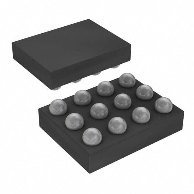
- Part No.:
- MAX20313EWC+
- Manufacturer:
- Analog Devices Inc./Maxim Integrated
- Category:
- Current Regulation/Management
- Package:
- 12-WFBGA, WLBGA
- Datasheet:
-
 MAX20313EWC+.pdf
- Description:
- IC CURRENT SWITCH 5% 12WLP
- Quantity:
- Payment:

- Shipping:

Inventory:1,095
Please send an inquiry. Send us your inquiry, and we will respond immediately.
Product details
Overview
MAX20313EWC+ from Maxim Integrated is a programmable current-limit switch designed for high-current load switching and large-capacitor charging in portable power rails. It features adjustable current limiting from 500mA to 6A, 10mΩ typical on-resistance, ±5% current-limit accuracy (2A–6A), and continuous current-limit fault response. It operates from +2.5V to +5.5V and supports RF power amplifier supply protection in smartphones.
For engineers reviewing the MAX20313EWC+ datasheet, MAX20313EWC+ pinout, MAX20313EWC+ application, or MAX20313EWC+ equivalent, key selection criteria include its active-high enable logic, continuous overcurrent response mode, reverse-current blocking with 3µs fast response, thermal self-limitation at +130°C, and WLP-12 package compatibility with space-constrained mobile designs.
Technical Context
The MAX20313EWC+ integrates a low-RON N-channel MOSFET with precision current-sense feedback and programmable blanking time (12–18ms) to distinguish transient surges from true faults. Its SETI pin accepts a resistor-to-GND to set current limit via a calibrated 3329 mV·Ω/A coefficient and 12 mA offset.
It implements dual reverse-current protection thresholds: accurate blocking triggers at 1–25mV (VOUT–VIN) with 128µs debounce, and fast blocking activates at 40–110mV with 3µs response. FLAG asserts open-drain upon overcurrent (after blanking), reverse fault, or thermal shutdown at +150°C.
Key Specifications
| Parameter | Value and Actual Design Meaning |
|---|---|
| Current Limit Range | 500mA to 6A, set by external RSETI (e.g., 680Ω = 6A); enables one device to cover multiple load profiles |
| On-Resistance (RON) | 10mΩ typical at 4.3V/1A; minimizes voltage drop and power loss in high-current paths |
| Current-Limit Accuracy | ±5% for 2A–6A range; ensures predictable fault threshold across temperature and supply voltage |
| Reverse Current Blocking | Fast response ≤3µs at ≥40mV VOUT–VIN; prevents backfeed into weak or shared power domains |
| Thermal Behavior | Self-limitation at +130°C (average current reduction), shutdown at +150°C with 20°C hysteresis; avoids PCB-level thermal runaway |
| Enable Logic | Active-high EN input (VIH ≥1.4V); simplifies direct interface with 1.8V/3.3V GPIO without level-shifting |
| Operating Voltage | +2.5V to +5.5V input range; supports USB PD, single-cell Li-ion, and dual-cell alkaline systems |
Pinout & Package
MAX20313EWC+ uses a 12-bump wafer-level package (WLP), 1.68mm × 1.48mm, 0.4mm pitch, RoHS-compliant. Bumps are on bottom; top-side marking is "ADT".
| Pin/Terminal | Circuit Role | Design Meaning |
|---|---|---|
| A1 | FLAG | Open-drain fault indicator; pulls low on overcurrent (after blanking), reverse current, or thermal shutdown |
| A2 | SETI | Current-limit programming input; connects to GND via resistor to set ILIM (500mA–6A); also provides current-monitor voltage |
| A3 | GND | Power and signal reference ground; must be low-impedance connection for stable current sensing |
| A4 | EN | Active-high enable; drives switch ON when ≥1.4V, OFF when ≤0.4V; no internal pullup/pulldown |
| B1, B4, C1, C4 | IN | Power input terminal; requires ≥1µF ceramic bypass close to package to suppress supply sag during short-circuit events |
| B2, B3, C2, C3 | OUT | Switched output terminal; connects to load; requires ≥1µF ceramic bypass to stabilize voltage during load transients |
Key Features
| Feature | Design Value |
|---|---|
| Adjustable current limit | 500mA–6A via single external resistor; eliminates need for multiple fixed-limit parts in BOM |
| Continuous current-limit mode | MAX20313EWC+ sustains regulated current during overload instead of latching off-enables auto-recovery in transient-fault environments |
| Fast reverse-current blocking | 3µs response at ≥40mV reverse bias; protects upstream supplies from backfeed in multi-rail systems |
| Thermal self-limitation | Automatic current reduction at +130°C junction; maintains functionality under sustained overload without shutdown |
| Accurate current monitoring | VSETI = (IOUT × 3329)/RSETI + 12mV; enables real-time load diagnostics without external sense resistor |
Applications
| RF Power Amplifier Supply | USB Type-C Port Power Switching |
|---|---|
|
Use Scenario: Isolating PA supply rail during transmit bursts to prevent supply droop and noise coupling into sensitive analog sections. IC Role / Device Role / Timing Role: High-side current-limit switch enabling controlled ramp-up and fast fault response to protect PA bias circuitry. Use Value: 10mΩ RON minimizes insertion loss; 3µs reverse-blocking prevents VBAT contamination from PA output harmonics. |
Use Scenario: Managing power delivery to USB-C receptacles with dynamic current allocation (e.g., 3A/5A modes) and overcurrent protection per port. IC Role / Device Role / Timing Role: Programmable load switch enforcing precise current limits aligned with USB PD contract negotiation. Use Value: ±5% current accuracy ensures compliance with USB PD 3.1 sink requirements; continuous mode avoids disruptive port resets during brief surges. |
| SDXC Card Power Management | UTCA/ATCA Board Slot Protection |
|
Use Scenario: Controlling power to high-capacity SDXC cards during hot-plug events and write-intensive operations. IC Role / Device Role / Timing Role: Inrush-limited switch preventing >1A surge into 1000µF+ card capacitance while maintaining stable VCCIO. Use Value: Adjustable 500mA–6A limit accommodates both legacy SDHC and UHS-II cards; 12–18ms blanking avoids false trips during card initialization. |
Use Scenario: Protecting backplane power slots in carrier-grade telecom blades against hot-swap transients and downstream short circuits. IC Role / Device Role / Timing Role: Robust current-limit switch with thermal self-regulation ensuring uninterrupted operation under sustained 3A–4A loads. Use Value: +130°C self-limitation allows safe operation without forced airflow; 72.8°C/W θJA enables thermal design on standard 4-layer boards. |
Equivalent & Alternatives
The following parts are listed as comparable options for similar current-limit switch applications.
| Alternative Part | Technical Difference | Application Difference | Selection Advice |
|---|---|---|---|
| MAX20315EWC+ | Same current range and RON, but active-low EN and continuous current-limit mode; identical thermal behavior and reverse-blocking specs | Requires inverted control signal; suitable where system MCU uses active-low enable outputs | Select MAX20315EWC+ only if board-level EN signal polarity matches-no change to current-limit or protection behavior |
| TPL7407LDR | Fixed 700mA limit, 120mΩ RON, no reverse-current blocking, no current monitoring, SOIC-8 package | Limited to low-current peripherals; lacks programmability and bidirectional protection needed for USB/PA rails | Use TPL7407LDR only for cost-sensitive, low-power non-critical loads where 700mA and SOIC layout are acceptable |
Compared with MAX20313EWC+, MAX20315EWC+ offers identical protection and current-setting capability but demands active-low control, whereas TPL7407LDR sacrifices adjustability, efficiency, and reverse protection for lower cost and simpler footprint-making MAX20313EWC+ optimal for compact, high-performance mobile and telecom power rails.
Availability
MAX20313EWC+ is available at Aetrix Electronics and suitable for RF power amplifier supply management, USB Type-C port protection, and SDXC card power sequencing requiring stable component supply, full production traceability, and long-term lifecycle support.
Supply support for MAX20313EWC+ includes scheduled delivery planning, volume procurement assistance, BOM continuity management, traceable sourcing, and lifecycle availability coordination for OEM customers, industrial embedded developers, connected-device designers, and electronics production programs.
Manufacturer
Maxim Integrated, now part of Analog Devices, designs precision analog, mixed-signal, and power-management ICs for demanding industrial, automotive, and communications applications.
The MAX20313–MAX20316 family targets space-constrained portable and infrastructure equipment requiring programmable, high-accuracy current limiting with integrated reverse-current and thermal protection-specifically optimized for smartphone PA rails, modular data cards, and telecom blade power distribution.
FAQ
What is the enable logic polarity of the MAX20313EWC+?
The MAX20313EWC+ uses active-high enable logic: the internal switch turns ON when the EN pin voltage exceeds 1.4V (VIH), and turns OFF when EN falls below 0.4V (VIL). This matches standard 1.8V/3.3V GPIO outputs without level-shifting. The MAX20313EWC+ does not include internal pull resistors on EN, so external pull-down is recommended for default-OFF behavior.
How do I set the current limit for the MAX20313EWC+?
Set the current limit for the MAX20313EWC+ by connecting a resistor (RSETI) between the SETI pin and GND. Use RSETI = 680Ω for 6A, 2050Ω for 2A, or 8350Ω for 500mA-values are listed in Table 2 of the datasheet. The relationship follows ILIM = (1.224V × 3329)/RSETI – 12mA. Do not use RSETI < 675Ω, as it disables protection.
Does the MAX20313EWC+ provide reverse-current protection?
Yes, the MAX20313EWC+ provides dual-mode reverse-current protection: accurate blocking triggers at 1–25mV (VOUT–VIN) with 128µs debounce, and fast blocking activates at 40–110mV with 3µs response. This prevents backfeed into source rails during hot-swap or multi-supply conflicts-critical for USB and SDXC applications where OUT may briefly exceed IN.
What happens during an overcurrent event on the MAX20313EWC+?
During an overcurrent event, the MAX20313EWC+ enters continuous current-limit mode: it regulates output current at the programmed ILIM value. After the blanking time (12–18ms), FLAG asserts low. If the overload persists, thermal self-limitation reduces average current at +130°C; at +150°C, thermal shutdown forces full OFF until junction cools by ~20°C. No latchoff occurs-recovery is automatic when load normalizes.
What package type and dimensions does the MAX20313EWC+ use?
The MAX20313EWC+ uses a 12-bump wafer-level package (WLP) measuring 1.68mm × 1.48mm with 0.4mm bump pitch. Top-side marking is "ADT". It requires micro-BGA land pattern per Maxim Application Note 1891 and JEDEC-standard reflow profile (peak 260°C). The WLP enables ultra-compact placement in smartphone and modem card layouts where QFN or SOIC are too large.
MAX20313EWC+ Specifications
- Product attributes
- Attribute value
- Manufacturer:
- Analog Devices Inc./Maxim Integrated
- Series:
- -
- Package/Case:
- 12-WFBGA, WLBGA
- Packaging:
- Strip
- Product Status:
- Active
- Function:
- Current Switch
- Sensing Method:
- -
- Accuracy:
- ±5%
- Voltage - Input:
- 2.5V ~ 5.5V
- Current - Output:
- 20mA
- Operating Temperature:
- -40°C ~ 85°C (TA)
- Grade:
- -
- Qualification:
- -
- Mounting Type:
- Surface Mount
- Supplier Device Package:
- 12-WLP (1.65x1.45)
MAX20313EWC+ FAQ
1.How can I place an order for MAX20313EWC+ through Aetrix?
Please submit a Request for Quotation (RFQ) for MAX20313EWC+ on Aetrix. Our sales agent will provide a competitive quotation and guide you through the order confirmation once you accept the terms.
2.Are the price and stock information for MAX20313EWC+ reliable?
The price and inventory of MAX20313EWC+ are updated periodically and may fluctuate due to market conditions. Stock and pricing data are typically refreshed every 24 hours. Quotation validity for MAX20313EWC+ is usually 5 days.
3.What payment methods are accepted for MAX20313EWC+?
We accept Wire Transfer, PayPal, Credit Card, Western Union, MoneyGram, and Escrow for MAX20313EWC+ transactions.
Note: Certain payment methods may incur a processing fee.
4.How is shipping managed for MAX20313EWC+?
MAX20313EWC+ orders can be shipped via leading logistics carriers, including DHL, UPS, FedEx, TNT, or Registered Mail.
Once your MAX20313EWC+ order is processed, you will receive an email with the shipment details and tracking number.
Note: Tracking information may take up to 24 hours to appear. Express delivery typically takes 3–5 business days.
5.How can I obtain technical support or documentation for MAX20313EWC+?
For technical support, including MAX20313EWC+ datasheets, pinout diagrams, or application guidance, please contact our engineering support team. They can provide detailed documentation and assistance for your MAX20313EWC+ requirements.
6.How does Aetrix verify that MAX20313EWC+ is sourced from the original manufacturer or authorized distributors?
All MAX20313EWC+ products on Aetrix are procured from qualified distributors and authorized channels. Our dedicated quality assurance team conducts strict verification, including traceability checks and, if necessary, third-party testing. This ensures that MAX20313EWC+ meets industry standards.
7.What is the process for return or replacement of MAX20313EWC+?
All MAX20313EWC+ units undergo pre-shipment inspection (PSI). If there is an issue with MAX20313EWC+, returns or replacements are accepted under the following conditions:
1.Quantity discrepancies, incorrect items, or visible external defects (such as breakage or corrosion), acknowledged by Aetrix.
2.The issue is reported within 90 days of delivery.
3.The MAX20313EWC+ part is unused and in its original packaging.
Return procedure for MAX20313EWC+:
1.Submit a request within 90 days.
2.Obtain a Return Material Authorization (RMA) from Aetrix.
MAX20313EWC+ Tags
.jpg)
-
PSSI2021SAY,115
Nexperia USA Inc.

-
BCR401RE6327HTSA1
Infineon Technologies

-
INA199B2DCKR
Texas Instruments
-
INA199A1DCKR
Texas Instruments
-
INA199B1DCKR
Texas Instruments
-
NSI45015WT1G
onsemi
-
NSI45020T1G
onsemi
-
NSI45030AT1G
onsemi
-
NSI45025AT1G
onsemi
-
NSI45020AT1G
onsemi
-
NSI50010YT1G
onsemi
-
LM334Z/NOPB
Texas Instruments
Tech Hub

A practical engineering guide to 3.3V and 5V logic compatibility, input thresholds, resistor dividers, translator ICs, MOSFET level shifting, I2C pull-ups, timing limits and power-sequencing risks.

The 74HC595 uses push-pull logic outputs, while the TPIC6B595 uses 50 V open-drain DMOS sinks for higher-power loads. This guide compares timing, current limits, 3.3 V interfacing, load wiring, thermal…

The 74HC595 converts serial data into eight stable parallel outputs. This guide covers pin functions, shift and storage timing, OE and MR behavior, drive-current limits, cascading, voltage compatibilit…

A technical comparison of level-sensitive latches and edge-triggered flip-flops, covering timing windows, setup and hold limits, master–slave operation, time borrowing, race-through, HDL inference and…

A D latch stores one bit while Enable controls when data can pass. This reference covers gate-level operation, truth tables, transparency, setup and hold timing, LE versus OE, common ICs and practical …

An SR latch stores one bit through cross-coupled feedback. This engineering reference covers NOR and NAND implementations, truth tables, forbidden-state recovery, gated operation, switch debouncing, fa…

Latch circuits retain one bit through feedback. This technical reference covers SR and D latches, truth tables, transparency, timing limits, latch-versus-flip-flop behavior, applications and common log…

An engineering guide to LED driver operation, constant-current and constant-voltage outputs, linear and switching topologies, dimming, IC selection, calculations, replacement compatibility, and fault c…

Operational amplifier guide covering op amp basics, feedback, ideal vs real op amps, common configurations, buffer circuits, offset, bias current, gain-bandwidth, slew rate, rail-to-rail limits and sel…

Jumper cables guide covering safe connection order, red and black clamp placement, final ground connection, cable gauge, length, clamp quality, copper vs CCA cables, jump starter comparison and battery…


