
 My Inquiry
 My Account


Analog Devices Inc./Maxim Integrated MAX2067ETL+T
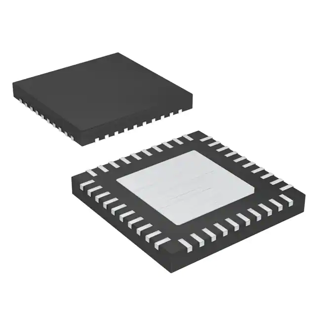
- Part No.:
- MAX2067ETL+T
- Manufacturer:
- Analog Devices Inc./Maxim Integrated
- Category:
- RF Amplifiers
- Package:
- 40-WFQFN Exposed Pad
- Datasheet:
-
 MAX2067ETL+T.pdf
- Description:
- IC AMP CELL 50MHZ-1GHZ 40TQFN
- Quantity:
- Payment:

- Shipping:

Inventory:1,303
Please send an inquiry. Send us your inquiry, and we will respond immediately.
Product details
Overview
MAX2067ETL+T from Maxim Integrated is a monolithic SiGe BiCMOS analog/digital variable-gain amplifier (VGA) designed for 50Ω RF systems operating from 50MHz to 1000MHz. It integrates an attenuator and amplifier with independent RF input/output ports, enabling configurable signal chain ordering (amplifier-first for NF optimization or amplifier-last for OIP3 optimization), +21.9dB typical gain, 4dB noise figure at maximum gain, and +43dBm output third-order intercept (OIP3) - making it suitable for base station IF/RF gain stages in LTE, WiMAX, and cable infrastructure.
For engineers reviewing the MAX2067ETL+T datasheet, MAX2067ETL+T pinout, MAX2067ETL+T application, or MAX2067ETL+T equivalent, key selection considerations include its dual-control interface (analog voltage or SPI-compatible 8-bit DAC), adjustable bias via RSET for linearity–current trade-off, guaranteed performance over –40°C to +85°C, and compact 40-pin thin QFN (6mm × 6mm) with exposed pad.
Technical Context
The MAX2067ETL+T implements a two-stage architecture: a programmable analog attenuator followed by a high-linearity driver amplifier, each with dedicated 50Ω RF ports. Its gain control supports both continuous analog voltage (0.25V–2.75V, –12.5dB/V slope) and digital SPI interface driving an on-chip 8-bit DAC (0–255 code range, 0.25V–2.75V output).
It operates from single +5V (HC mode: ICC = 123–146mA) or +3.3V (reduced performance: ICC = 60–82mA) supply, with external RSET resistor enabling bias current adjustment to optimize OIP3 vs. power consumption. Performance is characterized across temperature (–40°C to +85°C) and supply voltage variations, with full AC specs guaranteed under HC mode at +5V.
Key Specifications
| Parameter | Value and Actual Design Meaning |
|---|---|
| RF Frequency Range | 50MHz to 1000MHz - supports full-band operation in cellular, WiMAX, and DOCSIS-compliant CMTS applications without re-tuning. |
| Small-Signal Gain | +21.9dB (typ) at 200MHz - enables high dynamic range receiver front-end design with minimal external amplification. |
| Noise Figure | 4dB (typ) at max gain - ensures low degradation of system noise floor in sensitive receiver paths. |
| OIP3 | +43dBm (typ) at 200MHz, +5V HC mode - delivers robust linearity for multi-carrier LTE/WCDMA signals with minimal intermodulation distortion. |
| Gain Range | 31dB - provides wide dynamic control for AGC loops in transceivers and repeaters. |
| Supply Voltage | +5V (full performance) or +3.3V (reduced performance) - supports legacy 5V and modern low-voltage system integration. |
| DAC Resolution | 8-bit - enables precise 256-step gain control with <±0.1dB settling accuracy over full attenuation range. |
Pinout & Package
MAX2067ETL+T is housed in a 40-pin thin QFN package (6mm × 6mm) with exposed thermal pad (EP), optimized for RF performance and thermal dissipation in dense PCB layouts.
| Pin/Terminal | Circuit Role | Design Meaning |
|---|---|---|
| GND (Pins 1, 16, 19, 22, 24–28, 30, 31, 33–36) | Ground reference | Multiple low-inductance ground connections ensure stable RF return path and minimize supply noise coupling. |
| VREF_SELECT (Pin 2) | DAC reference select | Logic-high selects internal 2.5V DAC reference; logic-low enables external reference - critical for gain accuracy and temperature stability. |
| VDAC_EN (Pin 3) | DAC enable/disable | Disabling DAC disables digital control path, allowing pure analog VCTRL operation - simplifies fail-safe or hybrid control schemes. |
| DATA, CLK, CS (Pins 4–6) | SPI interface inputs | Standard 3-wire SPI allows daisy-chaining or individual addressing in multi-VGA systems; supports up to 20MHz clock for fast AGC response. |
| VDD_LOGIC (Pin 7) | Digital supply | Separate 1.8V–3.6V logic rail decoupled with 10nF capacitor - isolates digital switching noise from RF stages. |
| AMP_IN / AMP_OUT (Pins 20, 17) | Amplifier RF I/O | 50Ω-terminated differential-capable ports; require external matching only for non-50Ω source/load - simplifies integration into standard RF modules. |
| RSET (Pin 18) | Bias current setting | Resistor-to-ground sets amplifier quiescent current - enables tuning between +43dBm OIP3 (high-current) and lower power modes. |
| VCC_AMP (Pin 21) | Amplifier supply | +5V or +3.3V supply input with local bypassing - shared with attenuator supply; defines maximum linearity and gain capability. |
Key Features
| Feature | Design Value |
|---|---|
| Configurable signal chain order | Independent AMP_IN/AMP_OUT and ATTEN_IN/ATTEN_OUT ports allow physical reordering to prioritize either noise figure (amp first) or linearity (amp last) - no redesign needed. |
| On-chip 8-bit DAC with internal reference | Eliminates need for external DAC and reference ICs; 0.25V–2.75V output range matches optimal analog control voltage window for consistent gain slope. |
| Adjustable bias via RSET | Single external resistor tunes supply current from ~72mA to ~146mA (+5V), trading 1–2dB OIP3 for >30% power reduction - ideal for thermal-constrained designs. |
| 0.5dB gain flatness over 100MHz bandwidth | Ensures uniform channel response in wideband receivers (e.g., LTE 20MHz carriers), reducing equalization complexity in downstream DSP. |
| –70dBc HD2 / –87dBc HD3 | Ultra-low harmonic distortion preserves adjacent-channel integrity in full-duplex FDD systems and avoids interference in spectrum-sensitive deployments. |
Applications
| WCDMA/cdma2000 Base Stations | WiMAX/LTE Customer Premise Equipment |
|---|---|
|
Use Scenario: IF gain control in macrocell BTS receive path, compensating for antenna diversity combiner loss and variable feeder cable attenuation. IC Role / Device Role / Timing Role: Analog/digital VGA placed after LNA and before ADC, providing 31dB closed-loop AGC with <1µs response time. Use Value: Maintains constant ADC input level across 80dB dynamic range while preserving +43dBm OIP3 to prevent blocker-induced desensitization. |
Use Scenario: Transmit power control in outdoor WiMAX subscriber units, adapting output to regulatory limits and link budget changes. IC Role / Device Role / Timing Role: Final RF gain stage before PA driver, digitally controlled via SPI for fast TDD slot-based power ramping. Use Value: Enables precise +0.1dB gain resolution and <3.2µs analog control response - meeting ETSI spectral mask requirements during burst transmission. |
| Cable Modem Termination Systems (CMTS) | DOCSIS-Compliant EDGE QAM Modulation |
|
Use Scenario: Upstream receive path gain management in headend CMTS, handling multiple upstream channels (5–42MHz) with varying SNR. IC Role / Device Role / Timing Role: Programmable VGA in digitized upstream path, interfacing directly with 135MSPS ADC and supporting real-time AGC firmware. Use Value: 4dB NF ensures minimal degradation of upstream MER; 31dB range accommodates cable plant variations from 0dB to –35dB return loss. |
Use Scenario: Level-setting stage in video-on-demand edge QAM modulators, maintaining constant RF output across 64/256-QAM symbol rates and temperature drift. IC Role / Device Role / Timing Role: Post-modulator analog gain block, controlled by DAC voltage derived from D/A converter in FPGA-based modulator controller. Use Value: 0.5dB gain flatness over 100MHz prevents differential group delay in multi-channel QAM stacks; ±0.1dB gain repeatability ensures consistent MER across channels. |
Equivalent & Alternatives
The following parts are listed as comparable options for similar variable-gain amplifier applications.
| Alternative Part | Technical Difference | Application Difference | Selection Advice |
|---|---|---|---|
| MAX2065ETL+ | Pin-compatible family member with identical 40-pin QFN package and same 50–1000MHz range, but includes integrated analog/digital control and higher OIP3 (+45dBm) at expense of slightly higher ICC (150mA @ +5V). | Preferred where maximum linearity is prioritized over power efficiency - e.g., high-density macrocell BTS with active cooling. | Select MAX2065ETL+ when OIP3 margin > +43dBm is required and board space/power budget permits. |
| ADL5330ACPZ-R7 | 50–2000MHz GaAs VGA with 45dB gain range, but uses 3-wire serial interface (non-SPI), lacks on-chip DAC, and requires external reference; NF = 5.5dB, OIP3 = +40dBm. | Suitable for wider-bandwidth test equipment or broadband military comms where frequency coverage >1GHz is mandatory. | Choose ADL5330ACPZ-R7 only if 1–2GHz extension is essential and external DAC/reference circuitry is acceptable. |
Compared with MAX2065ETL+, the MAX2067ETL+ trades 2dB OIP3 for lower supply current and simplified biasing; versus ADL5330ACPZ-R7, it offers tighter gain flatness, integrated DAC, and SPI compatibility - making it optimal for cost- and size-constrained telecom infrastructure where 1GHz bandwidth suffices.
Availability
MAX2067ETL+T is available at Aetrix Electronics and suitable for WCDMA base stations, WiMAX CPE, and DOCSIS-compliant CMTS requiring stable component supply, long-term lifecycle support, and traceable sourcing for production ramp.
Supply support for MAX2067ETL+T includes scheduled delivery planning, volume procurement assistance, BOM continuity management, traceable sourcing, and lifecycle availability coordination for OEM customers, industrial embedded developers, connected-device designers, and electronics production programs.
Manufacturer
Maxim Integrated (now part of Analog Devices) is a semiconductor company specializing in high-performance analog, mixed-signal, and RF solutions for communications, industrial, and automotive markets.
The MAX2067ETL+T belongs to Maxim's high-linearity RF VGA product line, engineered specifically for demanding wireless infrastructure applications requiring wide dynamic range, low distortion, and flexible digital/analog control in compact form factors.
FAQ
What is the primary function of the MAX2067ETL+T in an RF signal chain?
The MAX2067ETL+T functions as a high-linearity, serial/analog-controlled variable-gain amplifier (VGA) that provides precise, wide-range gain adjustment (31dB) for 50Ω RF systems from 50MHz to 1000MHz. Its dual-stage architecture - with separate attenuator and amplifier sections - allows configuration to optimize either noise figure (amplifier-first) or linearity (amplifier-last), making it ideal for receiver and transmitter gain control in base stations and broadband infrastructure. The MAX2067ETL+T integrates an on-chip 8-bit DAC and supports both SPI and analog voltage control.
Can the MAX2067ETL+T operate from a +3.3V supply, and how does performance differ from +5V operation?
Yes, the MAX2067ETL+T supports single +3.3V supply operation with slightly reduced performance: typical gain drops to +21.3dB, OIP3 decreases to +38dBm, and noise figure increases to 4.3dB - all measured at 200MHz in high-current mode. Supply current reduces to 60–82mA. This mode is suitable for power-constrained applications where minor linearity/NF trade-offs are acceptable. Full +5V performance remains available for maximum dynamic range. The MAX2067ETL+T maintains guaranteed operation across –40°C to +85°C in both supply configurations.
How does the RSET pin affect the MAX2067ETL+T's performance and power consumption?
The RSET pin on the MAX2067ETL+T sets the amplifier's quiescent bias current via an external resistor to ground, enabling direct trade-off between linearity and power. A lower RSET value increases current, raising OIP3 (e.g., +43dBm at ~146mA with +5V) but increasing heat; a higher RSET reduces current (e.g., ~72mA), lowering OIP3 by ~1–2dB while cutting power by >30%. This adjustment is fully characterized and supported across temperature - allowing designers to tune the MAX2067ETL+T for specific thermal or efficiency targets without changing layout or firmware.
What is the significance of the MAX2067ETL+T's 0.5dB gain flatness specification?
The 0.5dB gain flatness over any 100MHz bandwidth (e.g., 200–300MHz or 800–900MHz) means the MAX2067ETL+T introduces minimal amplitude variation across wide modulation bandwidths - critical for maintaining signal fidelity in multi-carrier LTE, WCDMA, or OFDM systems. This flatness reduces the need for complex digital pre-distortion or analog equalization downstream, improves EVM consistency across channels, and ensures predictable AGC behavior in wideband receivers. It reflects tight process control and matched internal transistor characteristics within the MAX2067ETL+T's SiGe BiCMOS process.
Does the MAX2067ETL+T support both analog and digital gain control simultaneously, and how are they coordinated?
No - the MAX2067ETL+T supports analog control (via ANALOG_VCTRL pin) or digital control (via SPI-driven on-chip DAC), but not simultaneous use. The VDAC_EN pin enables or disables the DAC path; when disabled, only analog voltage controls gain. When enabled, the DAC output drives the same internal control node, overriding analog input. This design prevents conflict and ensures deterministic behavior: firmware can seamlessly switch between modes (e.g., coarse digital steps + fine analog trim), and the MAX2067ETL+T guarantees monotonic, repeatable gain response in either mode across temperature and supply voltage.
MAX2067ETL+T Specifications
- Product attributes
- Attribute value
- Manufacturer:
- Analog Devices Inc./Maxim Integrated
- Series:
- -
- Package/Case:
- 40-WFQFN Exposed Pad
- Packaging:
- Tape & Reel (TR)
- Product Status:
- Active
- Frequency:
- 50MHz ~ 1GHz
- P1dB:
- 18.7dBm
- Gain:
- 21.3dB
- Noise Figure:
- 4.2dB
- RF Type:
- Cellular, CDMA, GSM
- Voltage - Supply:
- 3V ~ 3.6V, 4.75V ~ 5.25V
- Current - Supply:
- 123mA
- Test Frequency:
- 350MHz
- Grade:
- -
- Qualification:
- -
- Mounting Type:
- Surface Mount
- Supplier Device Package:
- 40-TQFN (6x6)
MAX2067ETL+T FAQ
1.How can I place an order for MAX2067ETL+T through Aetrix?
Please submit a Request for Quotation (RFQ) for MAX2067ETL+T on Aetrix. Our sales agent will provide a competitive quotation and guide you through the order confirmation once you accept the terms.
2.Are the price and stock information for MAX2067ETL+T reliable?
The price and inventory of MAX2067ETL+T are updated periodically and may fluctuate due to market conditions. Stock and pricing data are typically refreshed every 24 hours. Quotation validity for MAX2067ETL+T is usually 5 days.
3.What payment methods are accepted for MAX2067ETL+T?
We accept Wire Transfer, PayPal, Credit Card, Western Union, MoneyGram, and Escrow for MAX2067ETL+T transactions.
Note: Certain payment methods may incur a processing fee.
4.How is shipping managed for MAX2067ETL+T?
MAX2067ETL+T orders can be shipped via leading logistics carriers, including DHL, UPS, FedEx, TNT, or Registered Mail.
Once your MAX2067ETL+T order is processed, you will receive an email with the shipment details and tracking number.
Note: Tracking information may take up to 24 hours to appear. Express delivery typically takes 3–5 business days.
5.How can I obtain technical support or documentation for MAX2067ETL+T?
For technical support, including MAX2067ETL+T datasheets, pinout diagrams, or application guidance, please contact our engineering support team. They can provide detailed documentation and assistance for your MAX2067ETL+T requirements.
6.How does Aetrix verify that MAX2067ETL+T is sourced from the original manufacturer or authorized distributors?
All MAX2067ETL+T products on Aetrix are procured from qualified distributors and authorized channels. Our dedicated quality assurance team conducts strict verification, including traceability checks and, if necessary, third-party testing. This ensures that MAX2067ETL+T meets industry standards.
7.What is the process for return or replacement of MAX2067ETL+T?
All MAX2067ETL+T units undergo pre-shipment inspection (PSI). If there is an issue with MAX2067ETL+T, returns or replacements are accepted under the following conditions:
1.Quantity discrepancies, incorrect items, or visible external defects (such as breakage or corrosion), acknowledged by Aetrix.
2.The issue is reported within 90 days of delivery.
3.The MAX2067ETL+T part is unused and in its original packaging.
Return procedure for MAX2067ETL+T:
1.Submit a request within 90 days.
2.Obtain a Return Material Authorization (RMA) from Aetrix.
MAX2067ETL+T Tags

-
BGU8019X
NXP USA Inc.
-
BGU8009,115
NXP USA Inc.
-
BGA725L6E6327FTSA1
Infineon Technologies
-
BGA123N6E6327XTSA1
Infineon Technologies
-
BGA125N6E6327XTSA1
Infineon Technologies
-
BGA855N6E6327XTSA1
Infineon Technologies
-
BGU7005,115
NXP USA Inc.
-
BGA524N6E6327XTSA1
Infineon Technologies

-
BGA824N6E6329XTSA1
Infineon Technologies
-
SKY65404-31
Skyworks Solutions Inc.
-
SKY65405-21
Skyworks Solutions Inc.
-
BGB741L7ESDE6327XTSA1
Infineon Technologies
Tech Hub

An engineering guide to LED driver operation, constant-current and constant-voltage outputs, linear and switching topologies, dimming, IC selection, calculations, replacement compatibility, and fault c…

Operational amplifier guide covering op amp basics, feedback, ideal vs real op amps, common configurations, buffer circuits, offset, bias current, gain-bandwidth, slew rate, rail-to-rail limits and sel…

Jumper cables guide covering safe connection order, red and black clamp placement, final ground connection, cable gauge, length, clamp quality, copper vs CCA cables, jump starter comparison and battery…

LDO regulator guide covering low dropout voltage, power dissipation, thermal design, PSRR, output noise, capacitor stability, adjustable LDO circuits, LDO vs buck converter and datasheet selection chec…

Conditional Access Module guide covering CAM meaning, CI/CI+ interface, smart card authorization, DVB security workflow, TV and set-top box compatibility, internal electronics, ESD protection, connecto…

Guide to electronic component obsolescence covering EOL risk, PCN/PDN notices, last-time buy planning, replacement options, form-fit-function validation, counterfeit risk and BOM lifecycle management.

18650 battery guide covering lithium-ion cell basics, 3.6V/3.7V voltage, 4.2V charging, mAh and Wh capacity, protected cells, chargers, BMS, series-parallel packs, holders, welding and sourcing checks.…

Hall effect sensor guide covering working principle, linear and digital sensors, Arduino circuits, current sensing, speed detection, automotive applications, A3144 examples, signal filtering and datash…

Product Change Notification guide for electronic components, covering PCN meaning, PCN vs PDN/EOL, common change types, risk levels, form-fit-function review, engineering validation, BOM control, LTB/L…

A practical guide to blend door actuators, covering HVAC function, symptoms, location, AC and heater issues, reset and calibration, replacement cost, electrical diagnosis, compatibility checks, and rep…


