
 My Inquiry
 My Account


Analog Devices Inc./Maxim Integrated MAX2105CWI
- Part No.:
- MAX2105CWI
- Manufacturer:
- Analog Devices Inc./Maxim Integrated
- Category:
- Unclassified
- Package:
- Datasheet:
-
 MAX2105CWI.pdf
- Description:
- TUNER IC DIRECT-CONV DBS 28-SOIC
- Quantity:
- Payment:

- Shipping:

Inventory:7,259
Please send an inquiry. Send us your inquiry, and we will respond immediately.
Product details
Overview
The MAX2105CWI from Maxim Integrated is a direct-conversion tuner IC for digital DBS satellite receivers, performing L-band RF-to-baseband I/Q downconversion across 950MHz–2150MHz. It integrates an LNA with 41dB AGC range, on-chip quadrature LO generation, dual downconverter mixers, and baseband amplifiers delivering 2.7Vp-p swing. Designed for cost-sensitive set-top box tuners, it enables low-noise system design when paired with a high-gain external LNA.
For engineers reviewing the MAX2105CWI datasheet, MAX2105CWI pinout, MAX2105CWI application, or MAX2105CWI equivalent, key selection criteria include its 41dB AGC range (vs. MAX2102's 50dB), -60dBm minimum input sensitivity, 15.5dB noise figure at 2141MHz, 6.5dBm input IP3 at 1450MHz, and 28dB RFIN-to-LO isolation - all critical for DVB-compliant DBS tuner front-end design.
Technical Context
The MAX2105CWI implements a broadband bipolar direct-conversion architecture with integrated 90° quadrature generator and dual-modulus prescaler (/64, /65), eliminating external phase-splitting components. Its RF front end features automatic gain control referenced to AGC voltage (1V–4V), enabling precise single-carrier power tracking from -60dBm to -19dBm per tone.
Baseband signal path includes offset-correction amplifiers with 0.22µF external capacitors on IDC/IDC/QDC/QDC pins, IOUT/QOUT outputs with 4.7Ω output impedance and ±1Ω matching, and 94MHz baseband bandwidth. LO input accepts differential or single-ended drive (-15dBm typical), with worst-case VSWR of 1.75:1 over band.
Key Specifications
| Parameter | Value and Actual Design Meaning |
|---|---|
| RF Input Range | 950MHz to 2150MHz - covers full L-band DBS spectrum including Ku-band downconverted signals |
| AGC Range | 41dB - supports input power from -60dBm to -19dBm while maintaining 0.5Vp-p baseband output |
| Noise Figure | 15.5dB at 2141MHz - optimized for high-sensitivity reception in weak-signal DBS environments |
| Input IP3 | 6.5dBm at 1450MHz - ensures robust two-tone intermodulation performance in multi-channel satellite systems |
| Baseband Bandwidth | 94MHz - supports wideband QPSK demodulation without aliasing when driving 100Ω AC-coupled loads |
| I/Q Imbalance | 0.5dB amplitude / 3° phase - maintains EVM integrity for DVB-S/QPSK constellations |
| Supply Voltage | +4.75V to +5.25V - compatible with standard 5V industrial power rails and tolerant of ripple up to 50mVp-p |
Pinout & Package
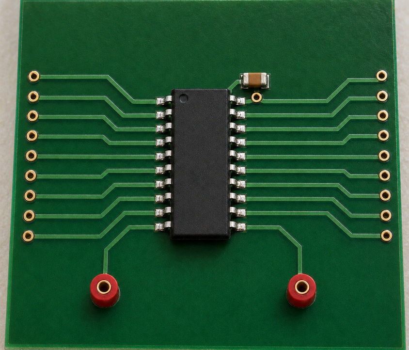
MAX2105CWI is housed in a 28-pin SO (Small Outline) package with exposed pad thermal enhancement. Pin assignments follow industry-standard RF tuner layout conventions, with dedicated RF, baseband, and supply domains separated to minimize coupling.
| Pin/Terminal | Circuit Role | Design Meaning |
|---|---|---|
| RFIN / RFIN | RF differential input pair | Accepts 50Ω source via 22pF AC coupling; requires external 51Ω termination on RFIN for balanced operation |
| IOUT / QOUT | Baseband differential outputs | Drive AC-coupled 100Ω loads; 2.7Vp-p clipping level supports ADC interface without external gain |
| AGC | Analog AGC control input | Voltage-controlled gain setting (1V–4V); bias current ±180µA enables servo-loop integration with baseband processor |
| IDC / IDC / QDC / QDC | Offset correction network terminals | Connect 0.22µF capacitors locally to null DC offsets; placement critical for <0.1° quadrature stability |
| LO / LO | Differential LO input ports | Accept -15dBm differential drive; 1.75:1 VSWR allows flexible synthesizer interface without external matching |
| VCC (pins 1,4,6,14,20,23,28) | Multiple supply rails | Dedicated VCC per functional block (RF, baseband, prescaler) minimizes supply-induced crosstalk and improves PSRR |
Key Features
| Feature | Design Value |
|---|---|
| On-chip quadrature LO generation | Eliminates external polyphase filter or transformer, reducing BOM count and layout area by >30% vs. discrete solutions |
| Integrated prescaler (/64, /65) | Enables direct connection to low-frequency reference clocks; eliminates need for external divider in low-cost synthesizer designs |
| Automatic baseband offset correction | Maintains <1mV DC offset at IOUT/QOUT under temperature drift and process variation, preserving QPSK constellation accuracy |
| Easy interface to MAX1002/MAX1003 ADCs | Matched 100Ω output impedance and 0.5Vp-p nominal level align directly with MAX1002's 125mVp-p–1Vp-p input range |
| Single +5V supply operation | Reduces system power architecture complexity; quiescent current 150mA (MAX2102) / 195mA (MAX2105) at +25°C |
Applications
| DBS Set-Top Box Tuner | Wireless Local Loop Receiver |
|---|---|
Use Scenario: Reception of Ku-band satellite signals (950–2150MHz) after LNB downconversion in consumer STB units. IC Role / Device Role / Timing Role: Direct RF-to-baseband I/Q downconverter with integrated AGC and quadrature LO generation. Use Value: Enables single-chip tuner front end with 41dB dynamic range, reducing component count versus IF-based architectures. | Use Scenario: Fixed wireless access point receiving 2.3–2.7GHz licensed band signals in rural broadband deployments. IC Role / Device Role / Timing Role: Broadband I/Q downconverter supporting flexible LO tuning across extended L-band. Use Value: 94MHz baseband bandwidth and 6.5dBm IP3 support high-data-rate QAM-64/256 modulation in interference-prone environments. |
| DVB-Compliant Satellite Modem | LMDS Base Station Front End |
Use Scenario: DVB-S2 receiver in professional broadcast equipment requiring ETSI EN 300 421 compliance. IC Role / Device Role / Timing Role: High-linearity tuner IC with 15.5dB noise figure and <3° I/Q phase imbalance. Use Value: Meets DVB-S2 BER requirements at low C/N ratios; offset correction maintains constellation stability over temperature. | Use Scenario: Local Multipoint Distribution Service base station operating in 27.5–29.5GHz band with harmonic-downconverted IF. IC Role / Device Role / Timing Role: L-band IF downconverter stage accepting 2nd-harmonic downconverted signals. Use Value: -32.3dBc spurious suppression and 28dB RFIN-to-LO isolation prevent co-channel interference from LO harmonics. |
Equivalent & Alternatives
The following parts are listed as comparable options for similar tuner IC applications.
| Alternative Part | Technical Difference | Application Difference | Selection Advice |
|---|---|---|---|
| MAX2102CWI | 50dB AGC range, -69dBm min input, 13.2dB NF at 1450MHz | Better sensitivity for ultra-low-signal DBS reception; higher NF degradation at band edges | Select MAX2102CWI when system-level noise figure dominates over external LNA gain trade-off |
| MAX2112ETJ+ | 3.3V operation, 1.2GHz–2.2GHz range, integrated PLL/VCO | Eliminates external LO source; reduced external component count but higher power (220mA) | Choose MAX2112ETJ+ for compact, self-contained tuner modules where board space is constrained |
Compared with MAX2102CWI and MAX2112ETJ+, the MAX2105CWI provides optimal balance of AGC headroom (41dB), external LNA compatibility, and 5V supply simplicity - making it ideal for cost-driven DBS STBs where system NF is managed upstream.
Availability
MAX2105CWI is available at Aetrix Electronics and suitable for DBS set-top boxes, wireless local loop receivers, DVB-compliant satellite modems, and LMDS base station front ends requiring stable component supply across production lifecycles.
Supply support for MAX2105CWI includes scheduled delivery planning, volume procurement assistance, BOM continuity management, traceable sourcing, and lifecycle availability coordination for OEM customers, industrial embedded developers, connected-device designers, and electronics production programs.
Manufacturer
Maxim Integrated (now part of Analog Devices) is a semiconductor company specializing in analog and mixed-signal ICs for power, interface, sensing, and RF applications.
The MAX210x tuner IC product line was designed specifically for cost-sensitive, high-volume digital satellite TV receivers - emphasizing direct-conversion architecture, integrated quadrature generation, and seamless interface to baseband ADCs like MAX1002/MAX1003.
FAQ
What is the operating temperature range for the MAX2105CWI?
The MAX2105CWI is rated for operation from 0°C to +70°C ambient temperature. This commercial-grade range aligns with typical indoor set-top box environments. The device's AGC performance, noise figure, and I/Q imbalance are fully characterized across this range, with worst-case phase imbalance shift of only ±0.6° over 0°C to +70°C - ensuring stable QPSK demodulation without recalibration.
Does the MAX2105CWI require external LO filtering?
No, the MAX2105CWI does not require external LO filtering due to its integrated oscillator buffer and on-chip quadrature generator. The LO input accepts either single-ended or differential drive (-15dBm typical), and internal limiting ensures consistent on-chip LO levels. However, differential LO routing with symmetrical traces is recommended to suppress LO leakage to RFIN, which is measured at -49dBm (typical) with single-ended drive.
How does the AGC range of MAX2105CWI compare to MAX2102CWI?
The MAX2105CWI has a 41dB AGC range (supporting -60dBm to -19dBm input), while the MAX2102CWI offers 50dB (supporting -69dBm to -19dBm). This 9dB reduction allows the MAX2105CWI to operate with higher front-end gain, enabling use of a high-gain external LNA to achieve lower overall system noise figure - a deliberate trade-off for improved sensitivity in noise-limited DBS applications.
Can the MAX2105CWI drive ADC inputs directly?
Yes, the MAX2105CWI can drive ADC inputs directly. Its IOUT and QOUT outputs deliver 0.5Vp-p nominal sine-wave levels into 100Ω AC-coupled loads, matching the input range of Maxim's MAX1002/MAX1003 dual ADCs. With 2.7Vp-p clipping level and 4.7Ω output impedance, it interfaces cleanly to anti-aliasing filters without external op-amps - simplifying signal chain design for DVB-S/QPSK demodulators.
Is the prescaler function enabled by default on MAX2105CWI?
No, the prescaler is disabled by default on MAX2105CWI. To disable it, leave PSGND (pin 25) open. Enabling requires connecting PSGND to ground and using MOD (pin 27) to select /64 or /65 division. Most DBS applications use external synthesizers (e.g., TSA5055) instead, avoiding prescaler-induced baseband spurs (~-20dBc) that could fall within the signal bandwidth.
MAX2105CWI Specifications
- Product attributes
- Attribute value
- Manufacturer:
- Analog Devices Inc./Maxim Integrated
- Series:
- -
- Packaging:
- Bulk
- Product Status:
- Obsolete
MAX2105CWI FAQ
1.How can I place an order for MAX2105CWI through Aetrix?
Please submit a Request for Quotation (RFQ) for MAX2105CWI on Aetrix. Our sales agent will provide a competitive quotation and guide you through the order confirmation once you accept the terms.
2.Are the price and stock information for MAX2105CWI reliable?
The price and inventory of MAX2105CWI are updated periodically and may fluctuate due to market conditions. Stock and pricing data are typically refreshed every 24 hours. Quotation validity for MAX2105CWI is usually 5 days.
3.What payment methods are accepted for MAX2105CWI?
We accept Wire Transfer, PayPal, Credit Card, Western Union, MoneyGram, and Escrow for MAX2105CWI transactions.
Note: Certain payment methods may incur a processing fee.
4.How is shipping managed for MAX2105CWI?
MAX2105CWI orders can be shipped via leading logistics carriers, including DHL, UPS, FedEx, TNT, or Registered Mail.
Once your MAX2105CWI order is processed, you will receive an email with the shipment details and tracking number.
Note: Tracking information may take up to 24 hours to appear. Express delivery typically takes 3–5 business days.
5.How can I obtain technical support or documentation for MAX2105CWI?
For technical support, including MAX2105CWI datasheets, pinout diagrams, or application guidance, please contact our engineering support team. They can provide detailed documentation and assistance for your MAX2105CWI requirements.
6.How does Aetrix verify that MAX2105CWI is sourced from the original manufacturer or authorized distributors?
All MAX2105CWI products on Aetrix are procured from qualified distributors and authorized channels. Our dedicated quality assurance team conducts strict verification, including traceability checks and, if necessary, third-party testing. This ensures that MAX2105CWI meets industry standards.
7.What is the process for return or replacement of MAX2105CWI?
All MAX2105CWI units undergo pre-shipment inspection (PSI). If there is an issue with MAX2105CWI, returns or replacements are accepted under the following conditions:
1.Quantity discrepancies, incorrect items, or visible external defects (such as breakage or corrosion), acknowledged by Aetrix.
2.The issue is reported within 90 days of delivery.
3.The MAX2105CWI part is unused and in its original packaging.
Return procedure for MAX2105CWI:
1.Submit a request within 90 days.
2.Obtain a Return Material Authorization (RMA) from Aetrix.
MAX2105CWI Tags

-
936106-1
TE Connectivity AMP Connectors
-
2050030-1
TE Connectivity AMP Connectors
-
1897255-2
TE Connectivity AMP Connectors
-
368811-1
TE Connectivity AMP Connectors
-
2296205-6
TE Connectivity AMP Connectors
-
2232228-1
TE Connectivity AMP Connectors
-
2296207-6
TE Connectivity AMP Connectors
-
2296206-8
TE Connectivity AMP Connectors
-
2316671-2
TE Connectivity AMP Connectors
-
2316671-4
TE Connectivity AMP Connectors
-
2316671-1
TE Connectivity AMP Connectors
-
174463-3
TE Connectivity AMP Connectors
Tech Hub
A D latch stores one bit while Enable controls when data can pass. This reference covers gate-level operation, truth tables, transparency, setup and hold timing, LE versus OE, common ICs and practical …

An SR latch stores one bit through cross-coupled feedback. This engineering reference covers NOR and NAND implementations, truth tables, forbidden-state recovery, gated operation, switch debouncing, fa…

Latch circuits retain one bit through feedback. This technical reference covers SR and D latches, truth tables, transparency, timing limits, latch-versus-flip-flop behavior, applications and common log…

An engineering guide to LED driver operation, constant-current and constant-voltage outputs, linear and switching topologies, dimming, IC selection, calculations, replacement compatibility, and fault c…

Operational amplifier guide covering op amp basics, feedback, ideal vs real op amps, common configurations, buffer circuits, offset, bias current, gain-bandwidth, slew rate, rail-to-rail limits and sel…

Jumper cables guide covering safe connection order, red and black clamp placement, final ground connection, cable gauge, length, clamp quality, copper vs CCA cables, jump starter comparison and battery…

LDO regulator guide covering low dropout voltage, power dissipation, thermal design, PSRR, output noise, capacitor stability, adjustable LDO circuits, LDO vs buck converter and datasheet selection chec…

Conditional Access Module guide covering CAM meaning, CI/CI+ interface, smart card authorization, DVB security workflow, TV and set-top box compatibility, internal electronics, ESD protection, connecto…

Guide to electronic component obsolescence covering EOL risk, PCN/PDN notices, last-time buy planning, replacement options, form-fit-function validation, counterfeit risk and BOM lifecycle management.

18650 battery guide covering lithium-ion cell basics, 3.6V/3.7V voltage, 4.2V charging, mAh and Wh capacity, protected cells, chargers, BMS, series-parallel packs, holders, welding and sourcing checks.…


