
 My Inquiry
 My Account


Analog Devices Inc./Maxim Integrated MAX2235EUP+T
- Part No.:
- MAX2235EUP+T
- Manufacturer:
- Analog Devices Inc./Maxim Integrated
- Category:
- RF Amplifiers
- Package:
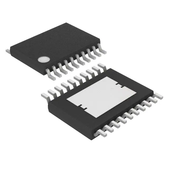
- 20-TSSOP (0.173", 4.40mm Width) Exposed Pad
- Datasheet:
-
 MAX2235EUP+T.pdf
- Description:
- IC AMP ISM 800MHZ-1GHZ 20TSSOP
- Quantity:
- Payment:

- Shipping:

Inventory:3,167
Please send an inquiry. Send us your inquiry, and we will respond immediately.
Product details
Overview
MAX2235EUP+T from Analog Devices is a silicon RF power amplifier optimized for 800–1000MHz constant-envelope systems, delivering +30dBm (1W) output at +3.6V with 47% power-added efficiency and 37dB gain-control range. It integrates autoramping, shutdown mode (<1μA), and direct OOK capability-designed for battery-powered 900MHz ISM-band transmitters in pagers and analog cellular handsets.
For engineers reviewing the MAX2235EUP+T datasheet, MAX2235EUP+T pinout, MAX2235EUP+T application, or MAX2235EUP+T equivalent, key selection criteria include its thermally enhanced 20-pin TSSOP-EP package, 836MHz-optimized matching, ramp capacitor-controlled turn-on/turn-off timing, and dual-mode bias control (SHDN/GC) enabling precise battery-life management in portable RF front-ends.
Technical Context
The MAX2235EUP+T implements a three-stage architecture: Class-A variable-gain input stage (37dB control range), Class-C driver stage, and Class-E power stage delivering 30dBm into 50Ω. Gain is monotonic with GC voltage (0.6V–2.3V), and bias sequencing is managed via SHDN and GC pins to support standby, active, and shutdown modes.
Its autoramping function uses an external capacitor between RAMP and REF (internally biased at 1.9V) to shape RF envelope rise/fall as a raised cosine-enabling clean OOK modulation without VCO pulling or intersymbol interference. Input and interstage matching networks are integrated on-die to maintain performance across 800–1000MHz.
Key Specifications
| Parameter | Value and Actual Design Meaning |
|---|---|
| Frequency Range | 800–1000MHz operational band; optimized for 836MHz with matched output network. |
| Output Power | +30dBm (1W) typical at +3.6V supply; +28dBm at +2.7V-supports single-cell Li-Ion and 3-cell NiCd operation. |
| Power-Added Efficiency | 47% typical at +30dBm output-minimizes thermal load and extends battery runtime in portable devices. |
| Gain Control Range | 37dB linear dB/V control via GC pin (0.6V–2.3V); enables dynamic output power adjustment without external attenuators. |
| Shutdown Current | <1μA typical-reduces system quiescent power during idle periods in intermittent transmission applications. |
| Ramp Control | External capacitor between RAMP and REF sets rise/fall time; supports OOK with <1.6mW/μs dP/dt and minimal spectral splatter. |
| Input VSWR | 1.5:1 at 50Ω source; remains stable in standby mode (ΔVSWR ≤1.5:1), simplifying antenna interface design. |
Pinout & Package
The MAX2235EUP+T is housed in a thermally enhanced 20-pin TSSOP-EP (exposed pad) package. The underside metal slug must be soldered directly to the PCB ground plane for optimal thermal dissipation and RF performance. Pin 13, 14, 17, 18, and the slug are all GND connections dedicated to the power stage.
| Pin/Terminal | Circuit Role | Design Meaning |
|---|---|---|
| 1 RFIN | RF Input | DC-blocked input to Class-A VGA stage; requires external series capacitor sized per operating frequency. |
| 2, 6, 7, 10, 13, 14, 17, 18, SLUG GND | Ground Reference | Dedicated low-inductance GND paths per functional block (input, driver, power stage); slug soldering mandatory for thermal integrity. |
| 3, 4, 5, 8, 9 VCC | Supply Inputs | Five separate VCC pins-each with dedicated bypassing (100pF/22pF/220pF + 1000pF)-isolate noise between input, bias, and power stages. |
| 11 RAMP | Ramp Timing Control | Connects to REF via external capacitor to generate controlled RF envelope rise/fall; determines OOK transition speed. |
| 12 REF | Ramp Reference | Internally regulated 1.9V reference for RAMP capacitor charging/discharging-no external regulation required. |
| 15, 16 RFOUT | RF Output | Differential-like output pair feeding external matching network; designed for 50Ω load at 836MHz with high-saturation current inductor. |
| 19 SHDN | Global Enable/Disable | Logic-high (>2.0V) enables operation; logic-low (<0.5V) forces full shutdown with <1μA ICC-critical for burst-mode power management. |
| 20 GC | Gain Control | Analog voltage input (0.6V–2.3V) setting VGA gain and final output power; monotonic dB/V response enables predictable closed-loop control. |
Key Features
| Feature | Design Value |
|---|---|
| Integrated Autoramping | Eliminates need for external ramp generators-external capacitor sets RF envelope timing for clean OOK transitions and reduced spectral splatter. |
| Multi-Stage Thermal Management | TSSOP-EP package with soldered slug and nine dedicated GND terminals ensures 6.4W continuous dissipation at +70°C ambient. |
| Three-Mode Bias Control | SHDN/GC combination enables On (full gain), Standby (input stage only, low ICC), and Shutdown (<1μA)-extending battery life in intermittent TX applications. |
| On-Chip Interstage Matching | Reduces external component count and board area-matching networks between VGA, driver, and power stage are integrated on-die. |
| Robust Load Mismatch Tolerance | Withstands 20:1 VSWR at +2.7V–+3.4V and 8:1 at +3.4V–+5.5V-enables reliable operation with imperfect antenna tuning or environmental detuning. |
Applications
| Two-Way Pagers | Analog Cellular Handsets |
|---|---|
|
Use Scenario: Battery-powered paging receivers requiring short-burst, high-integrity RF transmission in licensed 900MHz bands. IC Role / Device Role / Timing Role: Final-stage RF power amplifier driving antenna interface with autoramped OOK modulation. Use Value: +30dBm output and 47% PAE enable >10-hour battery life per charge; shutdown mode reduces standby drain to sub-μA levels. |
Use Scenario: Legacy AMPS handsets needing compact, efficient RF power delivery in mobile environments with variable supply voltage. IC Role / Device Role / Timing Role: High-efficiency PA supporting +2.7V to +5.5V operation and wide temperature range (-40°C to +85°C). Use Value: Single-supply flexibility accommodates aging battery profiles; integrated matching maintains consistent gain across 800–1000MHz band. |
| 900MHz ISM-Band Data Links | Microcellular GSM Power Class 5 |
|
Use Scenario: Low-cost wireless sensor networks transmitting telemetry bursts in unlicensed 902–928MHz spectrum. IC Role / Device Role / Timing Role: Autoramping PA enabling clean OOK without external filtering or VCO isolation components. Use Value: RAMP/REF capacitor control eliminates timing jitter in burst TX; 37dB gain range allows dynamic output scaling for link budget optimization. |
Use Scenario: Compact base station repeaters or femtocells requiring Class 5-compliant +30dBm output in microcell deployments. IC Role / Device Role / Timing Role: High-saturation PA stage delivering 1W into 50Ω with robust 20:1 load mismatch tolerance. Use Value: Exposed-pad TSSOP-EP package enables high-power density mounting; thermal design supports sustained +30dBm operation in enclosed enclosures. |
Equivalent & Alternatives
The following parts are listed as comparable options for similar RF power amplifier applications.
| Alternative Part | Technical Difference | Application Difference | Selection Advice |
|---|---|---|---|
| SX1231IMLTRT | Sub-GHz transceiver IC with integrated +17dBm PA; lacks discrete 1W output, autoramping, and external gain control. | Targeted at LoRa/Sigfox systems requiring integrated RX/TX-not suitable for standalone high-power OOK transmitters. | Select MAX2235EUP+T when discrete 1W output, analog GC control, and clean OOK envelope shaping are required. |
| RFM22BP | 868/915MHz transceiver with +20dBm integrated PA; no external ramp control, lower output power, and fixed gain architecture. | Designed for narrowband FSK/GFSK in industrial telemetry-not optimized for constant-envelope AMPS or pager protocols. | Choose MAX2235EUP+T for applications demanding >+28dBm output, 37dB analog gain range, and programmable autoramp timing. |
Compared with SX1231IMLTRT and RFM22BP, the MAX2235EUP+T provides higher output power (+30dBm vs. ≤+20dBm), true analog gain control (not digital register-based), and hardware-ramped OOK-making it uniquely suited for legacy 900MHz constant-envelope systems where spectral purity and battery efficiency are co-critical.
Availability
MAX2235EUP+T is available at Aetrix Electronics and suitable for two-way pagers, analog cellular handsets, 900MHz ISM-band data links, and microcellular GSM power-class applications requiring stable component supply across extended product lifecycles.
Supply support for MAX2235EUP+T includes scheduled delivery planning, volume procurement assistance, BOM continuity management, traceable sourcing, and lifecycle availability coordination for OEM customers, industrial embedded developers, connected-device designers, and electronics production programs.
Manufacturer
Analog Devices is a global leader in high-performance analog, mixed-signal, and RF ICs, serving industrial, communications, automotive, and aerospace markets with precision signal processing solutions.
The MAX2235EUP+T belongs to Analog Devices' RF power amplifier product line, engineered specifically for battery-efficient, spectrally clean transmission in 800–1000MHz constant-envelope communication systems.
FAQ
What is the maximum output power of the MAX2235EUP+T and at what supply voltage is it achieved?
The MAX2235EUP+T delivers +30dBm (1W) typical output power at +3.6V supply voltage, as verified under standard test conditions (fRFIN = 836MHz, TA = +25°C). At +2.7V, output drops to +28dBm-enabling compatibility with single-cell Li-Ion batteries while maintaining usable RF output. This performance is specified in the AC Electrical Characteristics table of the official MAX2235EUP+T datasheet.
How does the autoramping feature of the MAX2235EUP+T reduce spectral splatter in OOK applications?
The MAX2235EUP+T's autoramping shapes the RF envelope during turn-on and turn-off using a raised cosine profile, controlled by an external capacitor between RAMP and REF pins. This minimizes transient noise and harmonic distortion-reducing spectral splatter that would otherwise interfere with adjacent channels. Measured nonharmonic spurious output remains below -60dBc even under 6:1 load mismatch, confirming its suitability for strict OOK modulation standards.
What thermal management requirements apply to the MAX2235EUP+T package?
The MAX2235EUP+T uses a 20-pin TSSOP-EP package with an exposed metal slug that must be soldered directly to the PCB ground plane. All vias under the slug should be filled, and pins 13, 14, 17, and 18 must be connected to the slug via short traces. This configuration enables 6.4W continuous power dissipation at +70°C ambient and ensures junction temperature stays below +150°C under full +30dBm operation.
Can the MAX2235EUP+T operate from a 2.7V supply, and what performance trade-offs occur?
Yes, the MAX2235EUP+T operates over +2.7V to +5.5V. At +2.7V, output power is +28dBm (630mW) with 47% PAE maintained, but supply current increases to ~610mA at +30dBm-equivalent drive level. The device remains fully functional across the full -40°C to +85°C temperature range, making it viable for low-voltage battery systems-though peak output is reduced versus +3.6V operation.
What is the function of the GC pin on the MAX2235EUP+T, and how is it used in closed-loop power control?
The GC (Gain-Control) pin on the MAX2235EUP+T accepts an analog voltage (0.6V–2.3V) to set output power with monotonic dB/V response-verified across temperature. In closed-loop systems, a feedback detector monitors RFOUT and adjusts GC voltage via DAC or op-amp to maintain constant output despite supply or temperature drift. This replaces external attenuators and enables real-time power adaptation in dynamic RF environments.
MAX2235EUP+T Specifications
- Product attributes
- Attribute value
- Manufacturer:
- Analog Devices Inc./Maxim Integrated
- Series:
- -
- Package/Case:
- 20-TSSOP (0.173", 4.40mm Width) Exposed Pad
- Packaging:
- Tape & Reel (TR)
- Product Status:
- Active
- Frequency:
- 800MHz ~ 1GHz
- P1dB:
- -
- Gain:
- 26dB
- Noise Figure:
- -
- RF Type:
- ISM
- Voltage - Supply:
- 2.7V ~ 5.5V
- Current - Supply:
- 610mA
- Test Frequency:
- -
- Grade:
- -
- Qualification:
- -
- Mounting Type:
- Surface Mount
- Supplier Device Package:
- 20-TSSOP-EP
MAX2235EUP+T FAQ
1.How can I place an order for MAX2235EUP+T through Aetrix?
Please submit a Request for Quotation (RFQ) for MAX2235EUP+T on Aetrix. Our sales agent will provide a competitive quotation and guide you through the order confirmation once you accept the terms.
2.Are the price and stock information for MAX2235EUP+T reliable?
The price and inventory of MAX2235EUP+T are updated periodically and may fluctuate due to market conditions. Stock and pricing data are typically refreshed every 24 hours. Quotation validity for MAX2235EUP+T is usually 5 days.
3.What payment methods are accepted for MAX2235EUP+T?
We accept Wire Transfer, PayPal, Credit Card, Western Union, MoneyGram, and Escrow for MAX2235EUP+T transactions.
Note: Certain payment methods may incur a processing fee.
4.How is shipping managed for MAX2235EUP+T?
MAX2235EUP+T orders can be shipped via leading logistics carriers, including DHL, UPS, FedEx, TNT, or Registered Mail.
Once your MAX2235EUP+T order is processed, you will receive an email with the shipment details and tracking number.
Note: Tracking information may take up to 24 hours to appear. Express delivery typically takes 3–5 business days.
5.How can I obtain technical support or documentation for MAX2235EUP+T?
For technical support, including MAX2235EUP+T datasheets, pinout diagrams, or application guidance, please contact our engineering support team. They can provide detailed documentation and assistance for your MAX2235EUP+T requirements.
6.How does Aetrix verify that MAX2235EUP+T is sourced from the original manufacturer or authorized distributors?
All MAX2235EUP+T products on Aetrix are procured from qualified distributors and authorized channels. Our dedicated quality assurance team conducts strict verification, including traceability checks and, if necessary, third-party testing. This ensures that MAX2235EUP+T meets industry standards.
7.What is the process for return or replacement of MAX2235EUP+T?
All MAX2235EUP+T units undergo pre-shipment inspection (PSI). If there is an issue with MAX2235EUP+T, returns or replacements are accepted under the following conditions:
1.Quantity discrepancies, incorrect items, or visible external defects (such as breakage or corrosion), acknowledged by Aetrix.
2.The issue is reported within 90 days of delivery.
3.The MAX2235EUP+T part is unused and in its original packaging.
Return procedure for MAX2235EUP+T:
1.Submit a request within 90 days.
2.Obtain a Return Material Authorization (RMA) from Aetrix.
MAX2235EUP+T Tags

-
BGU8019X
NXP USA Inc.
-
BGU8009,115
NXP USA Inc.
-
BGA725L6E6327FTSA1
Infineon Technologies
-
BGA123N6E6327XTSA1
Infineon Technologies
-
BGA125N6E6327XTSA1
Infineon Technologies
-
BGA855N6E6327XTSA1
Infineon Technologies
-
BGU7005,115
NXP USA Inc.
-
BGA524N6E6327XTSA1
Infineon Technologies

-
BGA824N6E6329XTSA1
Infineon Technologies
-
SKY65404-31
Skyworks Solutions Inc.
-
SKY65405-21
Skyworks Solutions Inc.
-
BGB741L7ESDE6327XTSA1
Infineon Technologies
Tech Hub

An engineering guide to LED driver operation, constant-current and constant-voltage outputs, linear and switching topologies, dimming, IC selection, calculations, replacement compatibility, and fault c…

Operational amplifier guide covering op amp basics, feedback, ideal vs real op amps, common configurations, buffer circuits, offset, bias current, gain-bandwidth, slew rate, rail-to-rail limits and sel…

Jumper cables guide covering safe connection order, red and black clamp placement, final ground connection, cable gauge, length, clamp quality, copper vs CCA cables, jump starter comparison and battery…

LDO regulator guide covering low dropout voltage, power dissipation, thermal design, PSRR, output noise, capacitor stability, adjustable LDO circuits, LDO vs buck converter and datasheet selection chec…

Conditional Access Module guide covering CAM meaning, CI/CI+ interface, smart card authorization, DVB security workflow, TV and set-top box compatibility, internal electronics, ESD protection, connecto…

Guide to electronic component obsolescence covering EOL risk, PCN/PDN notices, last-time buy planning, replacement options, form-fit-function validation, counterfeit risk and BOM lifecycle management.

18650 battery guide covering lithium-ion cell basics, 3.6V/3.7V voltage, 4.2V charging, mAh and Wh capacity, protected cells, chargers, BMS, series-parallel packs, holders, welding and sourcing checks.…

Hall effect sensor guide covering working principle, linear and digital sensors, Arduino circuits, current sensing, speed detection, automotive applications, A3144 examples, signal filtering and datash…

Product Change Notification guide for electronic components, covering PCN meaning, PCN vs PDN/EOL, common change types, risk levels, form-fit-function review, engineering validation, BOM control, LTB/L…

A practical guide to blend door actuators, covering HVAC function, symptoms, location, AC and heater issues, reset and calibration, replacement cost, electrical diagnosis, compatibility checks, and rep…


