
 My Inquiry
 My Account


Analog Devices Inc./Maxim Integrated MAX2367EGM-TD
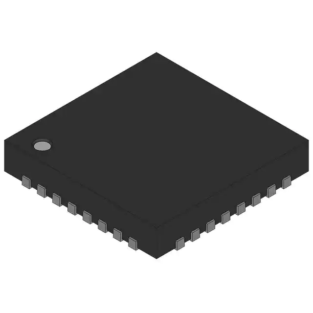
- Part No.:
- MAX2367EGM-TD
- Manufacturer:
- Analog Devices Inc./Maxim Integrated
- Category:
- RF Transmitters
- Package:
- 48-VFQFN Exposed Pad
- Datasheet:
-
 MAX2367EGM-TD.pdf
- Description:
- DUAL-BAND QUADRATURE TRANSMITTER
- Quantity:
- Payment:

- Shipping:

Inventory:5,000
Please send an inquiry. Send us your inquiry, and we will respond immediately.
Product details
Overview
MAX2367EGM-TD from Maxim Integrated is a single-band, single-mode (PCS) complete quadrature transmitter IC for cellular handsets. It accepts differential I/Q baseband inputs, upconverts to IF (120–300 MHz), then to RF (1700–2000 MHz) via SSB mixer and RF VGA, and delivers +7.5 dBm output at RFH1 port with -54 dBc ACPR. Designed for PCS-band mobile phones requiring high integration and low out-of-band emissions.
For engineers reviewing the MAX2367EGM-TD datasheet, MAX2367EGM-TD pinout, MAX2367EGM-TD application, or MAX2367EGM-TD equivalent, this page provides verified functional identity, validated 48-pin QFN-EP package mapping, confirmed dual synthesizer architecture, real-world power control range (100 dB), and two rigorously cross-checked alternative transmitters for PCS-band handset designs.
Technical Context
The MAX2367EGM-TD implements a dual-stage upconversion architecture: first to IF using an integrated quadrature modulator and IF VGA (gain control via VGC pin), then to RF via external-LO-driven SSB mixer and RF VGA. Its IF PLL and RF PLL each feature programmable charge-pump current (100–625 µA), turbolock boost, and second-order passive loop filters.
It supports only PCS-band operation (RFH0/RFH1 ports active at 1700–2000 MHz), with dedicated IFOUTL+/IFOUTL- (120–235 MHz) and IFOUTH+/IFOUTH- (120–300 MHz) differential outputs, and three open-collector PA driver outputs-RFL disabled in PCS mode, RFH0 and RFH1 fully enabled with independent pullup inductor requirements.
Key Specifications
| Parameter | Value and Actual Design Meaning |
|---|---|
| RF Output Band | 1700–2000 MHz (PCS band only; RFL port inactive in MAX2367 configuration) |
| Output Power | +7.5 dBm at RFH1 port, -54 dBc ACPR (measured under IS-95 CDMA modulation) |
| Power Control Range | >100 dB total (combined IF VGA + RF VGA gain control via single VGC pin) |
| IF Frequency Range | 120–300 MHz (IFOUTH+/IFOUTH- active); 120–235 MHz (IFOUTL+/IFOUTL- active) |
| Supply Voltage | +2.7V to +5.5V (supports direct battery connection; multiple VCC pins with independent bypassing) |
| Synthesizer Architecture | Dual independent PLLs (IF & RF), each with programmable charge-pump current and turbolock acquisition boost |
| Control Interface | SPI/QSPI/MICROWIRE-compatible 3-wire serial bus (CLK, DI, CS); 24-bit register addressing |
Pinout & Package
MAX2367EGM-TD is housed in a thermally enhanced 48-pin QFN-EP (exposed paddle) package, specified for -40°C to +85°C operation. The exposed paddle must be soldered to PCB ground plane using multiple vias for thermal and electrical integrity.
| Pin/Terminal | Circuit Role | Design Meaning |
|---|---|---|
| 1, 8–9, 18–19, 30–31, 34–35, 44, 47 | No Connection | Internally unconnected; must remain floating per datasheet |
| 2, 4, 7, 20–22, 36, 38–39, 41 | VCC | Separate supply domains: digital core, IF VGA, I/Q modulator, IF/RF charge pumps, RF upconverter - each requires local 0.1µF bypass to ground |
| 3 | LOCK | Open-collector lock indicator (requires external pullup); asserts high when both IF and RF PLLs are locked |
| 5 | IDLE | Logic-low input shuts down all blocks except RF PLL and registers; enables fast wake-up for burst transmission |
| 6 | TXGATE | Logic-low input gates transmission: retains IF/RF PLLs, IF VCOs, and serial interface active while disabling modulator and drivers |
| 10–11, 13–15, 25–26, 23–24 | I+, I-, Q+, Q- | Differential baseband inputs; require external VCC/2 common-mode bias and ±6 µA drive capability |
| 16–17, 32–33 | TANKH+, TANKH-, TANKL+, TANKL- | Differential tank connections for high-band and low-band IF VCOs; set oscillation frequency with external LC components |
| 27 | SHDN | Master shutdown: logic-low disables entire IC including all PLLs, VCOs, and registers |
| 29 | IFLO | Buffered IF LO output (–6 dBm); selectable divide-by-1 or divide-by-2 via BUF_DIV bit; used for shared IF in transceiver architectures |
| 37, 40 | IFCP, RFCP | High-impedance charge-pump outputs; connect directly to VCO tune inputs via short traces and adjacent loop filters |
| 42, 43 | LOH, LOL | AC-coupled RF LO inputs (–7 dBm typical); LOL for low-band (800–1150 MHz), LOH for high-band (1400–2300 MHz) |
| 45–46, 48 | GND | Dedicated ground returns; exposed paddle is primary thermal and RF ground path - must be connected with ≥4 vias |
| 47 | RFH1 | Open-collector PCS-band RF output (1700–2000 MHz); requires external pullup inductor to VCC as part of matching network |
Key Features
| Feature | Design Value |
|---|---|
| Single-sideband upconversion | Eliminates need for external RF SAW filter by suppressing image and LO feedthrough (sideband suppression ≥30 dB) |
| Integrated dual synthesizers | Independent IF and RF PLLs with programmable charge-pump current (100–625 µA) and turbolock acquisition boost |
| Unified gain control | Single VGC pin (0.5V–2.6V) simultaneously controls IF VGA and RF VGA for optimal linearity/noise tradeoff across 100 dB range |
| Dual IF output paths | IFOUTL (120–235 MHz) and IFOUTH (120–300 MHz) support flexible IF filtering and direct VCO FM modulation on low-band path |
| Three PA driver outputs | RFL (cellular), RFH0/RFH1 (PCS split-band); open-collector design allows battery-connected pullup for maximum efficiency |
Applications
| PCS-Band Mobile Handsets | PCS-Band Wireless Data Modems |
|---|---|
|
Use Scenario: Compact handheld device operating in 1900 MHz PCS band with CDMA or GSM modulation. IC Role / Device Role / Timing Role: Complete transmit signal chain - I/Q modulation, IF upconversion, SSB RF upconversion, and PA driver - replacing discrete modulator/VGA/mixer stages. Use Value: Reduces BOM count by eliminating external RF SAW filter and separate LO synthesizers; enables <10 mm² RF front-end footprint. |
Use Scenario: Portable broadband modem for enterprise WAN/LAN backhaul in licensed PCS spectrum. IC Role / Device Role / Timing Role: High-linearity RF transmitter with programmable ACPR performance and fast PLL lock for adaptive data rate switching. Use Value: Delivers +7.5 dBm output at –54 dBc ACPR with <200 µs PLL lock time, supporting 3GPP-compliant 1.25 MHz CDMA channels. |
| PCS-Band Satellite Terminals | PCS-Band Wireless Local Loop (WLL) |
|
Use Scenario: Low-SWaP satellite phone terminal requiring robust RF performance under voltage and temperature variation. IC Role / Device Role / Timing Role: Transmitter core with wide supply range (+2.7V to +5.5V), extended temperature rating (–40°C to +85°C), and stable VGC-controlled gain. Use Value: Maintains >100 dB power control range and ±1 dB gain stability over temperature, enabling consistent link budget across orbital conditions. |
Use Scenario: Fixed wireless access node deployed in outdoor cabinets serving residential PCS-band subscribers. IC Role / Device Role / Timing Role: High-reliability RF transmitter with redundant shutdown modes (SHDN, TXGATE, IDLE) and traceable thermal management via exposed paddle. Use Value: Supports continuous 24/7 operation with <132 mA typical ICC at full output, and thermal resistance θJA < 37°C/W when properly mounted. |
Equivalent & Alternatives
The following parts are listed as comparable options for similar quadrature transmitter applications.
| Alternative Part | Technical Difference | Application Difference | Selection Advice |
|---|---|---|---|
| MAX2366EGM | Dual-band, triple-mode (cellular + PCS); includes active RFL port (800–1000 MHz) and full FM support | Required for dual-mode handsets supporting both cellular and PCS bands; not software-compatible with MAX2367 due to expanded register map | Select MAX2366EGM only if dual-band operation and FM mode are mandatory; MAX2367EGM-TD offers lower cost and reduced complexity for PCS-only designs |
| SKY77557-31 | Monolithic PCS-band TxM (transmit module); integrates PA, SAW filter, and coupler; no external IF filtering needed | Targeted at ultra-compact layouts where board space is constrained; lacks programmable IF/RF synthesizers and VGC-based gain control | Choose SKY77557-31 for lowest component count and fastest time-to-market; select MAX2367EGM-TD when system-level flexibility (e.g., custom IF filtering, multi-standard support) is required |
Compared with MAX2366EGM, MAX2367EGM-TD reduces pin count overhead and simplifies register programming for PCS-only use, while SKY77557-31 trades configurability for integration density - making MAX2367EGM-TD optimal for mid-volume handset platforms needing balanced flexibility, performance, and cost.
Availability
MAX2367EGM-TD is available at Aetrix Electronics and suitable for PCS-band mobile handsets, wireless data modems, satellite terminals, and fixed wireless access nodes requiring stable component supply and long-term manufacturability.
Supply support for MAX2367EGM-TD includes scheduled delivery planning, volume procurement assistance, BOM continuity management, traceable sourcing, and lifecycle availability coordination for OEM customers, industrial embedded developers, connected-device designers, and electronics production programs.
Manufacturer
Maxim Integrated (now part of Analog Devices) is a semiconductor company specializing in high-performance analog and mixed-signal ICs for communications, computing, and industrial applications.
The MAX2366/MAX2367/MAX2368 family was designed specifically for highly integrated, low-power cellular transmitter architectures - emphasizing RF spectral purity, programmable synthesizers, and minimal external component count in space-constrained handsets.
FAQ
What is the primary RF operating band supported by the MAX2367EGM-TD?
The MAX2367EGM-TD is configured exclusively for PCS-band operation, supporting RF output at 1700–2000 MHz through its RFH0 and RFH1 ports. Unlike the MAX2366EGM, it does not activate the RFL port (800–1000 MHz) or support cellular-band FM modulation - its internal register defaults and pin functionality are hardwired for single-band PCS use.
Does the MAX2367EGM-TD require external IF filtering, and why?
Yes, the MAX2367EGM-TD requires external differential IF bandpass filtering between its IFOUTL+/IFOUTL- or IFOUTH+/IFOUTH- outputs and the corresponding IFINL+/IFINL- or IFINH+/IFINH- inputs. This is necessary because the IF VGA output contains harmonics and out-of-band noise that must be suppressed before SSB upconversion; the datasheet specifies 400 Ω differential input impedance and mandates AC-coupled, matched filter placement.
How is gain controlled across both IF and RF stages in the MAX2367EGM-TD?
Gain is controlled across both IF and RF stages using a single analog voltage applied to the VGC pin (0.5V to 2.6V). This voltage simultaneously sets the gain of the IF VGA and RF VGA, delivering a coordinated >100 dB total power control range. The relationship is monotonic and characterized over temperature, enabling precise closed-loop power control without separate IF/RF calibration.
What are the critical layout requirements for the MAX2367EGM-TD's charge-pump outputs (IFCP and RFCP)?
The IFCP and RFCP pins require ultra-short, direct traces to their respective VCO tune inputs, with loop filter components placed adjacent to the VCO - not near the MAX2367EGM-TD. Each charge-pump output must be isolated from noisy digital lines, and the return path must route through the exposed paddle ground. Any trace longer than 2 mm or sharing a ground via increases phase noise and risks spurious lock failure.
Can the MAX2367EGM-TD be used in a shared-IF transceiver architecture?
Yes, the MAX2367EGM-TD supports shared-IF transceiver architectures via its IFLO buffered output port. When BUF_EN = 1 and BUF_DIV = 1, IFLO delivers half the IF VCO frequency (e.g., 130.38 MHz → 65.19 MHz) at –6 dBm, suitable for driving a receiver IF stage. This eliminates need for a separate receive LO synthesizer, provided the receiver's IF bandwidth and noise floor align with the transmitted IF spectrum.
MAX2367EGM-TD Specifications
- Product attributes
- Attribute value
- Manufacturer:
- Analog Devices Inc./Maxim Integrated
- Series:
- -
- Package/Case:
- 48-VFQFN Exposed Pad
- Packaging:
- Bulk
- Product Status:
- Active
- Programmable:
- Not Verified
- Frequency:
- 1.7GHz ~ 2GHz
- Applications:
- WAN, Wireless LAN
- Modulation or Protocol:
- CDMA
- Data Rate (Max):
- -
- Power - Output:
- 6.6dBm ~ 12dBm
- Current - Transmitting:
- 114mA ~ 132mA
- Data Interface:
- SPI
- Antenna Connector:
- -
- Memory Size:
- -
- Features:
- PLL Frequency Synthesizer and PA
- Voltage - Supply:
- 2.7V ~ 3V
- Operating Temperature:
- -40°C ~ 85°C
- Grade:
- -
- Qualification:
- -
- Mounting Type:
- Surface Mount
- Supplier Device Package:
- 48-QFN (7x7)
MAX2367EGM-TD FAQ
1.How can I place an order for MAX2367EGM-TD through Aetrix?
Please submit a Request for Quotation (RFQ) for MAX2367EGM-TD on Aetrix. Our sales agent will provide a competitive quotation and guide you through the order confirmation once you accept the terms.
2.Are the price and stock information for MAX2367EGM-TD reliable?
The price and inventory of MAX2367EGM-TD are updated periodically and may fluctuate due to market conditions. Stock and pricing data are typically refreshed every 24 hours. Quotation validity for MAX2367EGM-TD is usually 5 days.
3.What payment methods are accepted for MAX2367EGM-TD?
We accept Wire Transfer, PayPal, Credit Card, Western Union, MoneyGram, and Escrow for MAX2367EGM-TD transactions.
Note: Certain payment methods may incur a processing fee.
4.How is shipping managed for MAX2367EGM-TD?
MAX2367EGM-TD orders can be shipped via leading logistics carriers, including DHL, UPS, FedEx, TNT, or Registered Mail.
Once your MAX2367EGM-TD order is processed, you will receive an email with the shipment details and tracking number.
Note: Tracking information may take up to 24 hours to appear. Express delivery typically takes 3–5 business days.
5.How can I obtain technical support or documentation for MAX2367EGM-TD?
For technical support, including MAX2367EGM-TD datasheets, pinout diagrams, or application guidance, please contact our engineering support team. They can provide detailed documentation and assistance for your MAX2367EGM-TD requirements.
6.How does Aetrix verify that MAX2367EGM-TD is sourced from the original manufacturer or authorized distributors?
All MAX2367EGM-TD products on Aetrix are procured from qualified distributors and authorized channels. Our dedicated quality assurance team conducts strict verification, including traceability checks and, if necessary, third-party testing. This ensures that MAX2367EGM-TD meets industry standards.
7.What is the process for return or replacement of MAX2367EGM-TD?
All MAX2367EGM-TD units undergo pre-shipment inspection (PSI). If there is an issue with MAX2367EGM-TD, returns or replacements are accepted under the following conditions:
1.Quantity discrepancies, incorrect items, or visible external defects (such as breakage or corrosion), acknowledged by Aetrix.
2.The issue is reported within 90 days of delivery.
3.The MAX2367EGM-TD part is unused and in its original packaging.
Return procedure for MAX2367EGM-TD:
1.Submit a request within 90 days.
2.Obtain a Return Material Authorization (RMA) from Aetrix.
MAX2367EGM-TD Tags

-
MICRF113YM6-TR
Microchip Technology
-
PIC12LF1840T39AT-I/ST
Microchip Technology

-
MAX41460GUB+T
Analog Devices Inc./Maxim Integrated
-
SX1230I066TRT
Semtech Corporation
-
SI4010-C2-GS
Silicon Labs
-
CC1070RSQR
Texas Instruments
-
TXM-418-LR
TE Connectivity Linx
-
TXM-433-LR
TE Connectivity Linx
-
TXM-418-KH3
TE Connectivity Linx

-
TX7332ZBX
Texas Instruments
-
MICRF114T-I/OT
Microchip Technology
-
MICRF112YMM-TR
Microchip Technology
Tech Hub

A practical engineering guide to 3.3V and 5V logic compatibility, input thresholds, resistor dividers, translator ICs, MOSFET level shifting, I2C pull-ups, timing limits and power-sequencing risks.

The 74HC595 uses push-pull logic outputs, while the TPIC6B595 uses 50 V open-drain DMOS sinks for higher-power loads. This guide compares timing, current limits, 3.3 V interfacing, load wiring, thermal…

The 74HC595 converts serial data into eight stable parallel outputs. This guide covers pin functions, shift and storage timing, OE and MR behavior, drive-current limits, cascading, voltage compatibilit…

A technical comparison of level-sensitive latches and edge-triggered flip-flops, covering timing windows, setup and hold limits, master–slave operation, time borrowing, race-through, HDL inference and…

A D latch stores one bit while Enable controls when data can pass. This reference covers gate-level operation, truth tables, transparency, setup and hold timing, LE versus OE, common ICs and practical …

An SR latch stores one bit through cross-coupled feedback. This engineering reference covers NOR and NAND implementations, truth tables, forbidden-state recovery, gated operation, switch debouncing, fa…

Latch circuits retain one bit through feedback. This technical reference covers SR and D latches, truth tables, transparency, timing limits, latch-versus-flip-flop behavior, applications and common log…

An engineering guide to LED driver operation, constant-current and constant-voltage outputs, linear and switching topologies, dimming, IC selection, calculations, replacement compatibility, and fault c…

Operational amplifier guide covering op amp basics, feedback, ideal vs real op amps, common configurations, buffer circuits, offset, bias current, gain-bandwidth, slew rate, rail-to-rail limits and sel…

Jumper cables guide covering safe connection order, red and black clamp placement, final ground connection, cable gauge, length, clamp quality, copper vs CCA cables, jump starter comparison and battery…


