
 My Inquiry
 My Account


Analog Devices Inc./Maxim Integrated MAX2371ETC+T
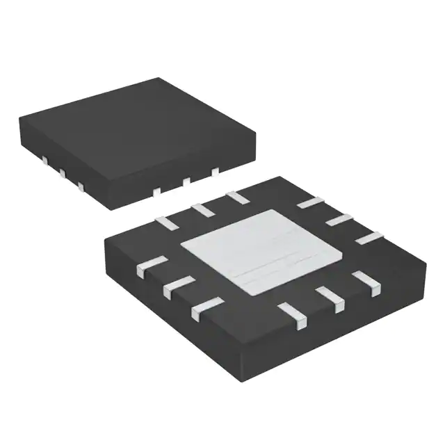
- Part No.:
- MAX2371ETC+T
- Manufacturer:
- Analog Devices Inc./Maxim Integrated
- Category:
- RF Amplifiers
- Package:
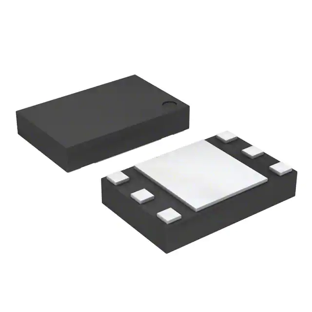
- 12-WFQFN Exposed Pad
- Datasheet:
-
 MAX2371ETC+T.pdf
- Description:
- IC RF AMP GPS 100MHZ-1GHZ 12TQFN
- Quantity:
- Payment:

- Shipping:

Inventory:1,549
Please send an inquiry. Send us your inquiry, and we will respond immediately.
Product details
Overview
MAX2371ETC+T from Maxim Integrated is a wideband single-channel low-noise amplifier (LNA) with integrated 20dB step attenuator and continuous AGC, designed for direct conversion receiver (DCR) front-ends operating from 100MHz to 1GHz. It delivers 15dB nominal small-signal gain, 1.8dB typical noise figure, and 40dB reverse isolation in a 12-pin TQFN-EP package, enabling high-dynamic-range RF signal conditioning in cellular base stations and ISM-band receivers.
For engineers reviewing the MAX2371ETC+T datasheet, MAX2371ETC+T pinout, MAX2371ETC+T application, or MAX2371ETC+T equivalent, this page provides verified circuit role, frequency-specific S-parameter behavior, AGC voltage-to-gain transfer function, LNA bias configuration modes, and real-world matching network constraints derived from Maxim's EV kit reference design and production characterization data.
Technical Context
The MAX2371ETC+T implements a single-ended RF input stage with exponential AGC control and digitally selectable gain modes via LNA_I and RF_ATTN pins. Its internal architecture integrates an RF attenuator, VGA core, and AGC amplifier with independent supply rails (RF_VCC and LNA_VCC), enabling simultaneous optimization of noise figure (1.8dB typ at 150MHz) and linearity (IIP3 = –10.5dBm min).
It operates across two distinct bands: low-band (136–174MHz) optimized by 33nH emitter inductor, and high-band (850–940MHz) requiring 2.5nH; both supported by external matching networks. Gain control spans 45dB AGC range plus 20dB step attenuation, achieving up to 60dB total dynamic range while maintaining stable S11 (< –10dB) and S12 (> –35dB) over temperature.
Key Specifications
| Parameter | Value and Actual Design Meaning |
|---|---|
| Noise Figure | 1.8dB typical at 150MHz - enables high sensitivity in weak-signal DCR applications without degrading SNR |
| Small-Signal Gain | 15dB nominal - provides sufficient first-stage amplification before mixer in low-IF architectures |
| Frequency Range | 100MHz to 1GHz - supports VHF/UHF/ISM bands with band-specific matching per EV kit guidelines |
| AGC Range | 45dB excluding step attenuator - allows precise RF level management across varying signal conditions |
| Step Attenuation | 20dB - improves system IP3 by ~18dB in strong-signal environments to suppress intermodulation |
| Supply Voltage | 2.65V to 3.3V - compatible with modern low-voltage RF subsystems and battery-powered receivers |
| Reverse Isolation | 40dB - prevents LO leakage re-radiation and maintains receiver stability in shared-antenna systems |
Pinout & Package
MAX2371ETC+T uses a 12-pin 3mm × 3mm TQFN-EP package (T1233+3) with exposed pad for thermal dissipation. Pin numbering follows standard top-view orientation with pin 1 at bottom-left corner.
| Pin/Terminal | Circuit Role | Design Meaning |
|---|---|---|
| 1 LNA_IN | RF Input | Single-ended RF port requiring DC-blocking capacitor and 50Ω matching network; S11 < –10dB at 150MHz |
| 2 LNA_E | LNA Emitter | Connects to GND via band-specific inductor (33nH for 150MHz); sets bias current and linearity trade-off |
| 3 RX_EN | LNA Enable | Active-high digital control; disables LNA with <20µA quiescent current when low - enables transmit/receive switching |
| 4 RF_ATTN | Attenuator Control | High = low-gain mode (–20dB step); low = high-gain mode - configurable independently of AGC |
| 5 AGC | AGC Voltage Input | Analog control pin; 1.275V–2.175V range yields 14.5dB gain variation; linear dB/V response ±10% |
| 6 LNA_I | Bias Current Select | High = high-current mode (3.5mA, optimal NF/gain); low = low-current mode (2.5mA, reduced performance) |
| 7 LNA_OUT | RF Output | Open-collector output requiring pull-up inductor to LNA_VCC and 50Ω matching; S22 < –10dB at 150MHz |
| 8 LNA_VCC | AGC Amplifier Supply | Separate 2.65–3.3V rail for AGC block; bypassed with 1500pF capacitor per Maxim EV kit layout |
| 9 AGC_BYP | AGC Bypass | AC ground for AGC loop; capacitor value trades off response time vs. blocker rejection (e.g., 100pF–1nF) |
| 10 RSET | Bias Reference | Connects to GND via precision resistor (1.1kΩ typical); sets 50–100µA internal reference current |
| 11 RF_VCC | LNA Core Supply | Dedicated 2.65–3.3V rail for LNA transistor; bypassed with 1500pF capacitor close to pin |
| 12 GND / EP | Ground / Exposed Pad | Main signal and thermal ground; EP must connect to large PCB ground plane via ≥4 vias for thermal reliability |
Key Features
| Feature | Design Value |
|---|---|
| Low-noise front-end architecture | 1.8dB NF at 150MHz enables sub–10dB system noise figure in DCR designs with proper matching |
| Dual-mode gain control | Independent digital (RF_ATTN) and analog (AGC) control allows hybrid gain management for wide dynamic range |
| Band-flexible matching | Emitter inductor selection (33nH/2.5nH) and external matching enable operation across 136–174MHz or 850–940MHz bands |
| Thermal-aware packaging | TQFN-EP with exposed pad achieves ≤40°C/W junction-to-board thermal resistance under 3.5mA operation |
| Power-efficient shutdown | RX_EN pin reduces ICC to <20µA - supports battery-save modes in portable receivers without PCB redesign |
Applications
| Cellular Base Station Receiver | ISM Band Transceiver Front-End |
|---|---|
Use Scenario: Receives 150MHz VHF signals in multi-carrier base station with co-located transmitters generating strong out-of-band interferers. IC Role / Device Role / Timing Role: First-stage LNA providing 15dB gain and 1.8dB NF while rejecting adjacent channel energy via 40dB reverse isolation. Use Value: 20dB step attenuator engages during high-RF conditions to boost IIP3 by 18dB, preventing front-end compression and IM3 generation. | Use Scenario: Processes 915MHz ISM-band signals in smart metering gateway with variable signal strength due to antenna placement and environmental fading. IC Role / Device Role / Timing Role: Wideband LNA with 45dB AGC range dynamically adjusts gain to maintain constant IF level despite >60dB path loss variation. Use Value: Linear dB/V AGC response ensures predictable gain reduction across temperature (±2dB variation from –40°C to +85°C). |
| Direct Conversion Radio Architecture | Portable DVB-T Tuner Module |
Use Scenario: Used in zero-IF receiver where LO leakage must be minimized to avoid self-mixing and DC offset corruption. IC Role / Device Role / Timing Role: High-reverse-isolation LNA isolates antenna from mixer input, reducing LO feedthrough into RF path. Use Value: 40dB S12 suppression prevents >–30dBm LO leakage from saturating LNA input in compact PCB layouts. | Use Scenario: Enables battery-powered handheld TV tuner supporting 470–862MHz DVB-T channels with fast channel switching. IC Role / Device Role / Timing Role: Low-power LNA with RX_EN-controlled shutdown reduces system standby current by >99% between channel scans. Use Value: 2.5mA low-current mode (LNA_I = low) extends battery life while maintaining usable SNR in strong-signal urban reception. |
Equivalent & Alternatives
The following parts are listed as comparable options for similar low-noise amplifier applications.
| Alternative Part | Technical Difference | Application Difference | Selection Advice |
|---|---|---|---|
| MAX2373ETC+T | Optimized for 850–940MHz band; higher NF (1.13dB typ at 930MHz) but same pinout and control interface | Targeted at PCS/UMTS cellular bands rather than VHF; requires different emitter inductor (2.5nH vs. 33nH) | Select MAX2373ETC+T when operating above 800MHz; use identical PCB layout but revise matching network and LNA_E inductor |
| SKY65111-363LF | Fixed-gain GaAs pHEMT LNA (17dB gain, 1.3dB NF at 900MHz); no AGC or step attenuator; 6-pin SOT-363 package | Suitable for simpler receive chains without dynamic range control; lacks digital gain modes and analog AGC interface | Choose SKY65111-363LF for cost-sensitive, fixed-gain applications where 60dB dynamic range is unnecessary |
Compared with MAX2373ETC+T, the MAX2371ETC+T offers lower noise figure and better VHF-band performance but requires different matching components; compared with SKY65111-363LF, it provides full programmable gain control at the expense of higher BOM count and layout complexity.
Availability
MAX2371ETC+T is available at Aetrix Electronics and suitable for cellular infrastructure, ISM-band wireless sensors, DVB-T tuners, and direct-conversion radio receivers requiring stable component supply across industrial temperature ranges.
Supply support for MAX2371ETC+T includes scheduled delivery planning, volume procurement assistance, BOM continuity management, traceable sourcing, and lifecycle availability coordination for OEM customers, industrial embedded developers, connected-device designers, and electronics production programs.
Manufacturer
Maxim Integrated (now part of Analog Devices) designs precision analog and mixed-signal ICs for communications, industrial, and consumer applications, with emphasis on power efficiency and signal integrity.
The MAX2371ETC+T belongs to Maxim's RF front-end product line, engineered specifically for high-dynamic-range direct-conversion receivers where simultaneous low noise, high linearity, and programmable gain are critical.
FAQ
What is the recommended inductor value for LNA_E in MAX2371ETC+T when operating at 150MHz?
The recommended inductor value for LNA_E in MAX2371ETC+T at 150MHz is 33nH, as specified in Table 5 of the datasheet for the low-band VHF configuration. This value optimizes gain, noise figure, and input return loss (S11) in the 136–174MHz range. Using 33nH with the reference matching network from the MAX2371 EV kit achieves 1.8dB noise figure and >14dB gain at 150MHz. Deviations require re-characterization of S-parameters and noise parameters.
Does MAX2371ETC+T support true zero-IF receiver architectures without DC offset issues?
Yes, MAX2371ETC+T supports zero-IF architectures through its high reverse isolation (40dB S12) and differential-capable external matching, which minimizes LO leakage coupling into the RF input. While the device itself does not correct DC offset, its 40dB reverse isolation prevents LO feedthrough from corrupting the LNA input stage - a key prerequisite for stable zero-IF operation. System-level DC offset cancellation must still be implemented downstream, typically in the baseband processor.
How does the AGC voltage range map to gain control in MAX2371ETC+T?
In MAX2371ETC+T, the AGC pin accepts a 1.275V to 2.175V analog voltage that produces a linear dB/V gain response: 1.275V yields ~20dB gain, 1.575V yields ~7.7dB, 1.875V yields ~14.5dB, and 2.175V yields minimum gain (~0dB). The slope is 33dB/V ±10% over the specified control range. This mapping holds for both high- and low-current modes (LNA_I), though absolute gain values shift downward by ~2–3dB in low-current mode.
Can MAX2371ETC+T operate outside its specified 100MHz–1GHz frequency range?
MAX2371ETC+T can operate outside 100MHz–1GHz, but performance is not characterized or guaranteed beyond this range. At 50MHz, S11 degrades to –5dB and gain drops below 10dB; at 1.5GHz, noise figure rises to >3dB and reverse isolation falls below 30dB. Maxim explicitly states in Note 2 that operation outside the specified bands is possible but uncharacterized. For reliable performance, use only within 100–1000MHz and apply band-specific matching per the EV kit schematics.
What is the maximum allowable input power for MAX2371ETC+T in shutdown mode (RX_EN = low)?
When RX_EN = low, MAX2371ETC+T enters shutdown mode with ICC < 20µA, and the absolute maximum RF input power is +5dBm, as specified in the Absolute Maximum Ratings table. Exceeding this level risks permanent damage to the unprotected LNA input transistor, even when disabled. For systems with high-power TX/RX switching, an external RF switch or limiter is required upstream of MAX2371ETC+T to clamp input power during transmit bursts.
MAX2371ETC+T Specifications
- Product attributes
- Attribute value
- Manufacturer:
- Analog Devices Inc./Maxim Integrated
- Series:
- -
- Package/Case:
- 12-WFQFN Exposed Pad
- Packaging:
- Tape & Reel (TR)
- Product Status:
- Active
- Frequency:
- 100MHz ~ 1GHz
- P1dB:
- -
- Gain:
- 15dB
- Noise Figure:
- 1.8dB
- RF Type:
- General Purpose
- Voltage - Supply:
- 2.65V ~ 3.3V
- Current - Supply:
- 5.5mA
- Test Frequency:
- -
- Grade:
- -
- Qualification:
- -
- Mounting Type:
- Surface Mount
- Supplier Device Package:
- 12-TQFN (3x3)
MAX2371ETC+T FAQ
1.How can I place an order for MAX2371ETC+T through Aetrix?
Please submit a Request for Quotation (RFQ) for MAX2371ETC+T on Aetrix. Our sales agent will provide a competitive quotation and guide you through the order confirmation once you accept the terms.
2.Are the price and stock information for MAX2371ETC+T reliable?
The price and inventory of MAX2371ETC+T are updated periodically and may fluctuate due to market conditions. Stock and pricing data are typically refreshed every 24 hours. Quotation validity for MAX2371ETC+T is usually 5 days.
3.What payment methods are accepted for MAX2371ETC+T?
We accept Wire Transfer, PayPal, Credit Card, Western Union, MoneyGram, and Escrow for MAX2371ETC+T transactions.
Note: Certain payment methods may incur a processing fee.
4.How is shipping managed for MAX2371ETC+T?
MAX2371ETC+T orders can be shipped via leading logistics carriers, including DHL, UPS, FedEx, TNT, or Registered Mail.
Once your MAX2371ETC+T order is processed, you will receive an email with the shipment details and tracking number.
Note: Tracking information may take up to 24 hours to appear. Express delivery typically takes 3–5 business days.
5.How can I obtain technical support or documentation for MAX2371ETC+T?
For technical support, including MAX2371ETC+T datasheets, pinout diagrams, or application guidance, please contact our engineering support team. They can provide detailed documentation and assistance for your MAX2371ETC+T requirements.
6.How does Aetrix verify that MAX2371ETC+T is sourced from the original manufacturer or authorized distributors?
All MAX2371ETC+T products on Aetrix are procured from qualified distributors and authorized channels. Our dedicated quality assurance team conducts strict verification, including traceability checks and, if necessary, third-party testing. This ensures that MAX2371ETC+T meets industry standards.
7.What is the process for return or replacement of MAX2371ETC+T?
All MAX2371ETC+T units undergo pre-shipment inspection (PSI). If there is an issue with MAX2371ETC+T, returns or replacements are accepted under the following conditions:
1.Quantity discrepancies, incorrect items, or visible external defects (such as breakage or corrosion), acknowledged by Aetrix.
2.The issue is reported within 90 days of delivery.
3.The MAX2371ETC+T part is unused and in its original packaging.
Return procedure for MAX2371ETC+T:
1.Submit a request within 90 days.
2.Obtain a Return Material Authorization (RMA) from Aetrix.
MAX2371ETC+T Tags

-
BGU8019X
NXP USA Inc.
-
BGU8009,115
NXP USA Inc.
-
BGA725L6E6327FTSA1
Infineon Technologies
-
BGA123N6E6327XTSA1
Infineon Technologies
-
BGA125N6E6327XTSA1
Infineon Technologies
-
BGA855N6E6327XTSA1
Infineon Technologies
-
BGU7005,115
NXP USA Inc.
-
BGA524N6E6327XTSA1
Infineon Technologies

-
BGA824N6E6329XTSA1
Infineon Technologies
-
SKY65404-31
Skyworks Solutions Inc.
-
SKY65405-21
Skyworks Solutions Inc.
-
BGB741L7ESDE6327XTSA1
Infineon Technologies
Tech Hub

An engineering guide to LED driver operation, constant-current and constant-voltage outputs, linear and switching topologies, dimming, IC selection, calculations, replacement compatibility, and fault c…

Operational amplifier guide covering op amp basics, feedback, ideal vs real op amps, common configurations, buffer circuits, offset, bias current, gain-bandwidth, slew rate, rail-to-rail limits and sel…

Jumper cables guide covering safe connection order, red and black clamp placement, final ground connection, cable gauge, length, clamp quality, copper vs CCA cables, jump starter comparison and battery…

LDO regulator guide covering low dropout voltage, power dissipation, thermal design, PSRR, output noise, capacitor stability, adjustable LDO circuits, LDO vs buck converter and datasheet selection chec…

Conditional Access Module guide covering CAM meaning, CI/CI+ interface, smart card authorization, DVB security workflow, TV and set-top box compatibility, internal electronics, ESD protection, connecto…

Guide to electronic component obsolescence covering EOL risk, PCN/PDN notices, last-time buy planning, replacement options, form-fit-function validation, counterfeit risk and BOM lifecycle management.

18650 battery guide covering lithium-ion cell basics, 3.6V/3.7V voltage, 4.2V charging, mAh and Wh capacity, protected cells, chargers, BMS, series-parallel packs, holders, welding and sourcing checks.…

Hall effect sensor guide covering working principle, linear and digital sensors, Arduino circuits, current sensing, speed detection, automotive applications, A3144 examples, signal filtering and datash…

Product Change Notification guide for electronic components, covering PCN meaning, PCN vs PDN/EOL, common change types, risk levels, form-fit-function review, engineering validation, BOM control, LTB/L…

A practical guide to blend door actuators, covering HVAC function, symptoms, location, AC and heater issues, reset and calibration, replacement cost, electrical diagnosis, compatibility checks, and rep…


