
 My Inquiry
 My Account


Analog Devices Inc./Maxim Integrated MAX2373ETC+T
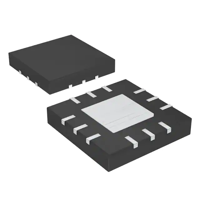
- Part No.:
- MAX2373ETC+T
- Manufacturer:
- Analog Devices Inc./Maxim Integrated
- Category:
- RF Amplifiers
- Package:
- 12-WFQFN Exposed Pad
- Datasheet:
-
 MAX2373ETC+T.pdf
- Description:
- IC AMP GPS 850MHZ-940MHZ 12TQFN
- Quantity:
- Payment:

- Shipping:

Inventory:2,321
Please send an inquiry. Send us your inquiry, and we will respond immediately.
Product details
Overview
The MAX2373ETC+T from Maxim Integrated is a single-channel, single-ended wideband low-noise amplifier (LNA) with switchable 20dB step attenuator and continuous automatic gain control (AGC), designed for 850–940MHz VLIF/DCR receiver front-ends. It delivers 15.5dB typical small-signal gain, 1.1dB typical noise figure at 900MHz, 45dB AGC range excluding step attenuation, and 40dB reverse isolation in a 12-pin TQFN-EP package.
For engineers reviewing the MAX2373ETC+T datasheet, MAX2373ETC+T pinout, MAX2373ETC+T application, or MAX2373ETC+T equivalent, this page provides verified RF performance data, validated gain-mode behavior, confirmed AGC voltage-to-dB transfer characteristics, and precise LNA biasing requirements for 900MHz band operation.
Technical Context
The MAX2373ETC+T implements a two-stage RF signal path: an input LNA core followed by a digitally controlled 20dB RF step attenuator and a continuously variable VGA stage driven by analog AGC voltage (0.8V to 2.6V). Its high/low-current modes (LNA_I pin) and high/low-gain modes (RF_ATTN pin) enable independent optimization of noise figure versus linearity across varying signal conditions.
It operates over 850–940MHz with external matching networks, uses separate LNA_VCC and RF_VCC supplies (2.65–3.3V), and features shutdown via RX_EN. The AGC loop maintains linear dB/V response (33dB/V typical) over its 45dB control range while preserving S11 < –10dB and S12 < –35dB across temperature.
Key Specifications
| Parameter | Value and Actual Design Meaning |
|---|---|
| Noise Figure | 1.1dB typical at 900MHz - enables high sensitivity in weak-signal cellular/WCDMA receivers |
| Small-Signal Gain | 15.5dB nominal at 900MHz - provides sufficient first-stage amplification before mixer |
| RF Frequency Range | 850–940MHz - optimized for PCS/UMTS Band V and Band VIII applications |
| AGC Range | 45dB excluding step attenuator - supports wide dynamic range without saturation in burst-mode systems |
| Step Attenuation | 19.5dB typical (RF_ATTN high→low) - allows fast 20dB gain reduction to handle strong interferers |
| Supply Current | 3.5mA typical (high-current mode), adjustable to 2.5mA - balances power vs. NF/IP3 trade-offs in battery-powered devices |
| Reverse Isolation | –42dB minimum (S12) - prevents LO leakage re-radiation and improves system stability |
Pinout & Package
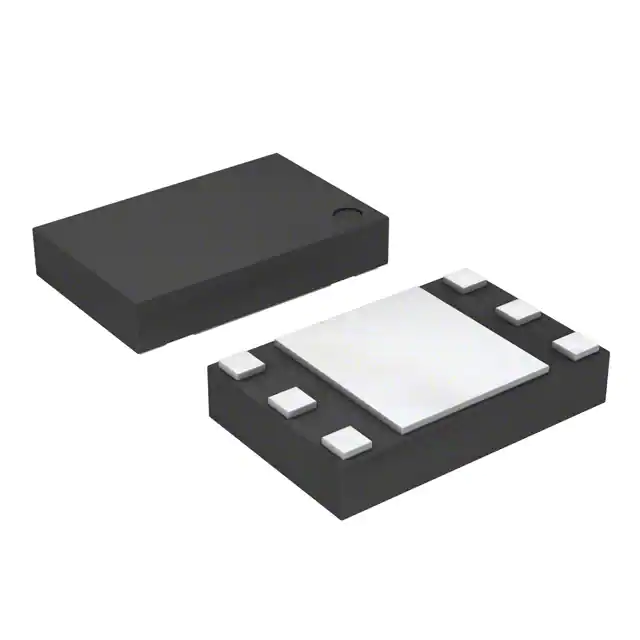
MAX2373ETC+T is housed in a 3mm × 3mm, 12-pin TQFN-EP package (T1233+3) with exposed pad for thermal dissipation. Pin 1 is LNA_IN; pin 12 is GND; EP is internally connected to GND and must be soldered to a large ground plane using multiple low-inductance vias.
| Pin/Terminal | Circuit Role | Design Meaning |
|---|---|---|
| 1 LNA_IN | RF Input | Requires DC-blocking capacitor and 50Ω-matched network; impedance varies minimally with gain/AGC state |
| 2 LNA_E | LNA Emitter | Connects to GND via 2.5nH inductor (for 800–1000MHz); sets bias current and linearity |
| 3 RX_EN | Enable Control | Active-high digital input; disables entire LNA when low, drawing only 20µA quiescent current |
| 4 RF_ATTN | Attenuator Mode | High = low-gain mode (–20dB step); low = high-gain mode; independent of AGC voltage |
| 5 AGC | Analog Gain Control | Voltage input (0.8–2.6V) controlling continuous VGA; 2.2V = ~10dB gain, 1.3V = ~55dB gain |
| 6 LNA_I | Bias Current Select | High = 3.5mA (optimal NF/IP3); low = 2.5mA (power saving); default = high if floating |
| 7 LNA_OUT | RF Output | Open-collector output requiring pull-up inductor to LNA_VCC and 50Ω match to next stage |
| 8 LNA_VCC | AGC Amplifier Supply | 2.65–3.3V supply for AGC circuitry; bypass with 100pF capacitor close to pin |
| 9 AGC_BYP | AGC Loop Filter | Connect 1–10nF capacitor to GND; sets AGC response time and blocker rejection bandwidth |
| 10 RSET | Bias Reference | Connect 1.1kΩ resistor to GND to set internal reference current (50–100µA) |
| 11 RF_VCC | LNA Core Supply | 2.65–3.3V supply for LNA transistor; bypass with 100pF capacitor; no tuned circuits allowed |
| 12 GND | Ground | Main signal ground; connects to EP; requires low-impedance return path for RF and AGC sections |
Key Features
| Feature | Design Value |
|---|---|
| Two independent gain control axes | RF_ATTN selects 20dB step; AGC pin provides 45dB continuous analog control - enables >60dB total dynamic range |
| Optimized 900MHz performance | 1.1dB NF, –12dBm IIP3, and –9dBm P1dB at 900MHz - meets stringent UMTS/WCDMA front-end linearity specs |
| Dual bias current modes | LNA_I pin toggles between 3.5mA (NF = 1.1dB) and 2.5mA (NF = 1.8dB) - supports adaptive power management |
| Robust reverse isolation | S12 ≤ –42dB across 850–940MHz - suppresses LO feedthrough and prevents oscillator pulling |
| Thermally enhanced package | TQFN-EP with exposed pad - achieves junction-to-board θJB < 40°C/W for sustained 3.5mA operation |
Applications
| Cellular Base Station Receiver | UMTS/WCDMA Handset Front-End |
|---|---|
Use Scenario: Receives 850–940MHz uplink signals in macro/micro base stations with high adjacent-channel interference. IC Role / Device Role / Timing Role: First-stage LNA providing high gain and low noise before downconversion; handles strong blockers via RF_ATTN + AGC coordination. Use Value: 45dB AGC range + 20dB step attenuation enables >60dB instantaneous dynamic range, meeting 3GPP ACLR requirements. | Use Scenario: Processes WCDMA Band V (824–849MHz) and Band VIII (880–915MHz) receive paths in mobile handsets. IC Role / Device Role / Timing Role: Single-chip LNA with integrated AGC and attenuation for compact, low-power direct-conversion architectures. Use Value: 1.1dB NF and 3.5mA supply current deliver best-in-class sensitivity-per-milliamp for extended battery life. |
| PCS Band Infrastructure Receiver | IoT Cellular Modem Front-End |
Use Scenario: Receives 1850–1910MHz PCS signals in small-cell access points where spectral purity is critical. IC Role / Device Role / Timing Role: High-linearity LNA stage with 2.5mA low-current mode activated during low-SINR conditions to reduce self-heating. Use Value: –12dBm IIP3 and 40dB reverse isolation minimize intermodulation distortion and prevent desensitization from nearby transmitters. | Use Scenario: Enables NB-IoT or LTE-M reception in space-constrained asset trackers operating on Band 8 (900MHz). IC Role / Device Role / Timing Role: Low-power, matched LNA with shutdown (RX_EN) for duty-cycled wake-up listening. Use Value: 20µA shutdown current and fast AGC settling (<1µs) support ultra-low average power in battery-operated IoT nodes. |
Equivalent & Alternatives
The following parts are listed as comparable options for similar LNA applications.
| Alternative Part | Technical Difference | Application Difference | Selection Advice |
|---|---|---|---|
| MAX2371ETC+T | Optimized for 136–174MHz VHF band; 0.82dB NF at 150MHz; 14.5dB gain; uses 33nH LNA_E inductor | Targeted at VHF DCRs (e.g., land-mobile radio), not 900MHz cellular bands | Select MAX2371ETC+T only for sub-200MHz applications requiring lower NF than MAX2373ETC+T offers at VHF |
| QPL9057TR13 | 50Ω-matched 5-pin SOT-563; 0.65dB NF at 900MHz; fixed 17.5dB gain; no AGC or step attenuator | Used in simpler receivers needing only fixed-gain LNA; lacks dynamic range control capability | Choose QPL9057TR13 when system-level AGC is handled externally and board space is constrained |
Compared with MAX2371ETC+T and QPL9057TR13, the MAX2373ETC+T uniquely combines 900MHz-optimized noise performance, integrated 20dB step attenuation, and 45dB analog AGC in a single chip-enabling compact, high-dynamic-range receiver designs without external gain-control components.
Availability
MAX2373ETC+T is available at Aetrix Electronics and suitable for cellular infrastructure, UMTS/WCDMA handset design, and IoT modem development requiring stable component supply and long-term manufacturability.
Supply support for MAX2373ETC+T includes scheduled delivery planning, volume procurement assistance, BOM continuity management, traceable sourcing, and lifecycle availability coordination for OEM customers, industrial embedded developers, connected-device designers, and electronics production programs.
Manufacturer
Maxim Integrated (now part of Analog Devices) is a semiconductor company specializing in high-performance analog, mixed-signal, and RF ICs for communications, computing, and industrial markets.
The MAX2373ETC+T belongs to Maxim's wideband LNA family targeting direct-conversion and VLIF receiver front-ends, with design focus on cellular/WCDMA frequency bands and integrated dynamic range control.
FAQ
What is the typical noise figure of the MAX2373ETC+T at 900MHz?
The MAX2373ETC+T has a typical noise figure of 1.1dB at 900MHz under standard test conditions (VCC = 2.775V, LNA_I = high, RF_ATTN = low, TA = +25°C). This value is confirmed in Table 4 of the official datasheet and reflects optimal biasing for low-noise operation in UMTS Band VIII applications. The MAX2373ETC+T maintains NF ≤ 1.3dB across its full 850–940MHz operating band.
How does the RF_ATTN pin affect gain and linearity in the MAX2373ETC+T?
The RF_ATTN pin on the MAX2373ETC+T selects between two discrete gain states: low-gain mode (RF_ATTN = high) reduces gain by ~19.5dB and improves IIP3 by ~18dB, while high-gain mode (RF_ATTN = low) maximizes sensitivity. This 20dB step is independent of AGC voltage and enables rapid strong-signal protection without degrading AGC loop stability. The MAX2373ETC+T datasheet specifies this behavior across temperature and supply voltage.
Can the MAX2373ETC+T operate outside its specified 850–940MHz band?
The MAX2373ETC+T is characterized and guaranteed for operation from 850MHz to 940MHz. While functional operation may occur outside this range (e.g., down to 700MHz or up to 1GHz), performance parameters-including noise figure, gain flatness, and reverse isolation-are not specified or tested beyond this band. Designers should rely only on the 850–940MHz data for production use; the MAX2373ETC+T datasheet explicitly notes that operation outside these frequencies has not been characterized.
What is the recommended inductor value for LNA_E in the MAX2373ETC+T for 900MHz operation?
For 900MHz operation, the MAX2373ETC+T requires a 2.5nH inductor connected between pin 2 (LNA_E) and ground, as specified in Table 5 of the datasheet under "800MHz" and "1GHz" entries. This value optimizes the trade-off between gain, noise figure, and input IP3. Using alternate values (e.g., 2.7nH or 1.8nH) shifts the center frequency and degrades 900MHz performance; the MAX2373ETC+T evaluation kit validates 2.5nH for Band VIII compliance.
Does the MAX2373ETC+T support true shutdown mode, and what is its quiescent current?
Yes, the MAX2373ETC+T supports full shutdown via the RX_EN pin: when RX_EN is driven low, the LNA core and AGC amplifier disable completely, reducing supply current to 20µA maximum (typical 5µA) while maintaining pin compatibility and state retention. This mode is fully specified in the Absolute Maximum Ratings and DC Electrical Characteristics tables, and is distinct from low-current mode (LNA_I = low), which draws 2.5mA. The MAX2373ETC+T datasheet confirms this behavior across –40°C to +85°C.
MAX2373ETC+T Specifications
- Product attributes
- Attribute value
- Manufacturer:
- Analog Devices Inc./Maxim Integrated
- Series:
- -
- Package/Case:
- 12-WFQFN Exposed Pad
- Packaging:
- Tape & Reel (TR)
- Product Status:
- Active
- Frequency:
- 850MHz ~ 940MHz
- P1dB:
- -19.5dBm
- Gain:
- 15.5dB
- Noise Figure:
- 1.8dB
- RF Type:
- General Purpose
- Voltage - Supply:
- 2.65V ~ 3.3V
- Current - Supply:
- 3.5mA
- Test Frequency:
- 850MHz ~ 940MHz
- Grade:
- -
- Qualification:
- -
- Mounting Type:
- Surface Mount
- Supplier Device Package:
- 12-TQFN (3x3)
MAX2373ETC+T FAQ
1.How can I place an order for MAX2373ETC+T through Aetrix?
Please submit a Request for Quotation (RFQ) for MAX2373ETC+T on Aetrix. Our sales agent will provide a competitive quotation and guide you through the order confirmation once you accept the terms.
2.Are the price and stock information for MAX2373ETC+T reliable?
The price and inventory of MAX2373ETC+T are updated periodically and may fluctuate due to market conditions. Stock and pricing data are typically refreshed every 24 hours. Quotation validity for MAX2373ETC+T is usually 5 days.
3.What payment methods are accepted for MAX2373ETC+T?
We accept Wire Transfer, PayPal, Credit Card, Western Union, MoneyGram, and Escrow for MAX2373ETC+T transactions.
Note: Certain payment methods may incur a processing fee.
4.How is shipping managed for MAX2373ETC+T?
MAX2373ETC+T orders can be shipped via leading logistics carriers, including DHL, UPS, FedEx, TNT, or Registered Mail.
Once your MAX2373ETC+T order is processed, you will receive an email with the shipment details and tracking number.
Note: Tracking information may take up to 24 hours to appear. Express delivery typically takes 3–5 business days.
5.How can I obtain technical support or documentation for MAX2373ETC+T?
For technical support, including MAX2373ETC+T datasheets, pinout diagrams, or application guidance, please contact our engineering support team. They can provide detailed documentation and assistance for your MAX2373ETC+T requirements.
6.How does Aetrix verify that MAX2373ETC+T is sourced from the original manufacturer or authorized distributors?
All MAX2373ETC+T products on Aetrix are procured from qualified distributors and authorized channels. Our dedicated quality assurance team conducts strict verification, including traceability checks and, if necessary, third-party testing. This ensures that MAX2373ETC+T meets industry standards.
7.What is the process for return or replacement of MAX2373ETC+T?
All MAX2373ETC+T units undergo pre-shipment inspection (PSI). If there is an issue with MAX2373ETC+T, returns or replacements are accepted under the following conditions:
1.Quantity discrepancies, incorrect items, or visible external defects (such as breakage or corrosion), acknowledged by Aetrix.
2.The issue is reported within 90 days of delivery.
3.The MAX2373ETC+T part is unused and in its original packaging.
Return procedure for MAX2373ETC+T:
1.Submit a request within 90 days.
2.Obtain a Return Material Authorization (RMA) from Aetrix.
MAX2373ETC+T Tags

-
BGU8019X
NXP USA Inc.
-
BGU8009,115
NXP USA Inc.
-
BGA725L6E6327FTSA1
Infineon Technologies
-
BGA123N6E6327XTSA1
Infineon Technologies
-
BGA125N6E6327XTSA1
Infineon Technologies
-
BGA855N6E6327XTSA1
Infineon Technologies
-
BGU7005,115
NXP USA Inc.
-
BGA524N6E6327XTSA1
Infineon Technologies

-
BGA824N6E6329XTSA1
Infineon Technologies
-
SKY65404-31
Skyworks Solutions Inc.
-
SKY65405-21
Skyworks Solutions Inc.
-
BGB741L7ESDE6327XTSA1
Infineon Technologies
Tech Hub

An engineering guide to LED driver operation, constant-current and constant-voltage outputs, linear and switching topologies, dimming, IC selection, calculations, replacement compatibility, and fault c…

Operational amplifier guide covering op amp basics, feedback, ideal vs real op amps, common configurations, buffer circuits, offset, bias current, gain-bandwidth, slew rate, rail-to-rail limits and sel…

Jumper cables guide covering safe connection order, red and black clamp placement, final ground connection, cable gauge, length, clamp quality, copper vs CCA cables, jump starter comparison and battery…

LDO regulator guide covering low dropout voltage, power dissipation, thermal design, PSRR, output noise, capacitor stability, adjustable LDO circuits, LDO vs buck converter and datasheet selection chec…

Conditional Access Module guide covering CAM meaning, CI/CI+ interface, smart card authorization, DVB security workflow, TV and set-top box compatibility, internal electronics, ESD protection, connecto…

Guide to electronic component obsolescence covering EOL risk, PCN/PDN notices, last-time buy planning, replacement options, form-fit-function validation, counterfeit risk and BOM lifecycle management.

18650 battery guide covering lithium-ion cell basics, 3.6V/3.7V voltage, 4.2V charging, mAh and Wh capacity, protected cells, chargers, BMS, series-parallel packs, holders, welding and sourcing checks.…

Hall effect sensor guide covering working principle, linear and digital sensors, Arduino circuits, current sensing, speed detection, automotive applications, A3144 examples, signal filtering and datash…

Product Change Notification guide for electronic components, covering PCN meaning, PCN vs PDN/EOL, common change types, risk levels, form-fit-function review, engineering validation, BOM control, LTB/L…

A practical guide to blend door actuators, covering HVAC function, symptoms, location, AC and heater issues, reset and calibration, replacement cost, electrical diagnosis, compatibility checks, and rep…


