
 My Inquiry
 My Account


Analog Devices Inc./Maxim Integrated MAX2612ETA/V+T
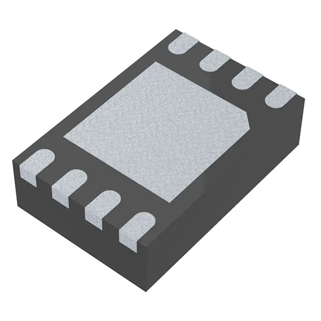
- Part No.:
- MAX2612ETA/V+T
- Manufacturer:
- Analog Devices Inc./Maxim Integrated
- Category:
- RF Amplifiers
- Package:
- 8-WFDFN Exposed Pad
- Datasheet:
-
 MAX2612ETA/V+T.pdf
- Description:
- IC RF AMP GPS 40MHZ-4GHZ 8TDFN
- Quantity:
- Payment:

- Shipping:

Inventory:3,421
Please send an inquiry. Send us your inquiry, and we will respond immediately.
Product details
Overview
MAX2612ETA/V+T from Maxim Integrated is a high-performance broadband RF gain block designed as a PA predriver or low-noise amplifier in 40MHz–4000MHz systems. It delivers +18.3dB gain at 1GHz, +18.2dBm P1dB output, 2.1–2.65dB noise figure at 2GHz, and +35.2dBm OIP3 - enabling robust signal amplification in cellular infrastructure and microwave radio front-ends.
For engineers reviewing the MAX2612ETA/V+T datasheet, MAX2612ETA/V+T pinout, MAX2612ETA/V+T application, or MAX2612ETA/V+T equivalent, key selection criteria include its AEC-Q100 qualified automotive grade, shutdown capability via EN pin, 2mm × 3mm TDFN-EP package with exposed thermal pad, and verified performance across -40°C to +85°C.
Technical Context
The MAX2612ETA/V+T employs a rugged bipolar Darlington architecture optimized for wideband linearity and input surge resilience, supporting up to +20dBm RF input without external protection. Its internally 50Ω-matched RFIN and RFOUT ports eliminate external matching networks across 40MHz–4GHz.
It features an enable-controlled shutdown mode (EN pin logic-low), drawing only 7µA in disable state, and operates from a single 3.0V–5.25V supply with 69mA typical supply current at VCC = 5V and TA = +25°C. Thermal design leverages θJA = 60°C/W and θJC = 11°C/W via the exposed pad.
Key Specifications
| Parameter | Value and Actual Design Meaning |
|---|---|
| Frequency Range | 40MHz to 4000MHz - supports full LTE, WiMAX, and microwave radio bands without re-tuning. |
| Small-Signal Gain | 18.3dB at 1GHz - provides stable, high gain for cascaded RF stages with minimal compensation. |
| OIP3 | +35.2dBm - enables high dynamic range in multi-tone environments like CATV and wireless LAN. |
| Noise Figure | 2.1–2.65dB at 2GHz - ensures low degradation of SNR in receiver LNA applications. |
| P1dB Output | +18.2dBm - delivers sufficient drive level for subsequent PA stages in compact transceivers. |
| Supply Voltage | 3.0V to 5.25V - compatible with standard 3.3V and 5V system rails without regulation overhead. |
| Shutdown Current | 7µA - enables power gating in battery-sensitive or duty-cycled RF modules. |
Pinout & Package
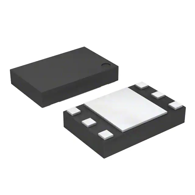
The MAX2612ETA/V+T is housed in an 8-pin, 2mm × 3mm TDFN-EP (Exposed Pad) package with RoHS-compliant lead-free finish. The exposed pad must be soldered to PCB ground via a 3×3 via array for optimal thermal dissipation (θJC = 11°C/W).
| Pin/Terminal | Circuit Role | Design Meaning |
|---|---|---|
| 1, 3, 6, 8 | GND | Ground reference for RF and DC paths; requires low-inductance connection to PCB ground plane. |
| 2 | RFIN | RF input port, internally matched to 50Ω; requires 0.01µF DC-blocking capacitor. |
| 4 | EN/RBIAS | Enable control input (logic-low disables amplifier); no bias resistor needed - fixed-bias operation. |
| 5 | VCC | DC supply input; requires local decoupling: 470pF + 10nF near pin + 10µF tantalum bulk cap (ESR > 2Ω). |
| 7 | RFOUT | RF output and DC feed point; connects to VCC via 220nH RF choke and to load via 0.01µF DC-blocking capacitor. |
| EP | Exposed Pad | Thermal and electrical ground; must be connected to PCB ground plane with multiple vias for thermal reliability. |
Key Features
| Feature | Design Value |
|---|---|
| Automotive qualification | AEC-Q100 Grade 3 certified (-40°C to +85°C), enabling use in infotainment, telematics, and ADAS RF modules. |
| Input overload resilience | +20dBm maximum RF input rating - eliminates need for external limiter or attenuator in burst-mode or transient-prone systems. |
| Gain flatness | ≤0.8dB variation from 1–4GHz - reduces calibration complexity in wideband receivers and spectrum analyzers. |
| ESD robustness | 2.5kV HBM rating - enhances manufacturing yield and field reliability in handling-sensitive RF assembly lines. |
| Thermal efficiency | 60°C/W junction-to-ambient thermal resistance on standard four-layer board - sustains +18.2dBm output under continuous operation at +85°C ambient. |
Applications
| Cellular Infrastructure | Microwave Radio |
|---|---|
Use Scenario: Small-cell base station receive path requiring wideband amplification across 700MHz–3.8GHz bands. IC Role / Device Role / Timing Role: Low-noise predriver stage before mixer or ADC, providing gain and noise figure optimization. Use Value: 2.1–2.65dB NF at 2GHz and +35.2dBm OIP3 preserve signal integrity in dense multi-carrier deployments. | Use Scenario: Point-to-point backhaul transceiver operating in 2.4GHz, 5.8GHz, or 24GHz licensed bands. IC Role / Device Role / Timing Role: Cascadable 50Ω gain block in IF or RF chain, enabling modular, scalable link budgets. Use Value: 40–4000MHz bandwidth and <0.8dB gain flatness simplify band-switching without recalibration. |
| Wireless LAN | Automotive Telematics |
Use Scenario: Dual-band 2.4/5GHz Wi-Fi 6 front-end module requiring high-linearity amplification. IC Role / Device Role / Timing Role: Transmit driver or diversity receive LNA in MIMO antenna subsystems. Use Value: +18.3dB gain and +35.2dBm OIP3 support concurrent multi-channel operation with low ACPR. | Use Scenario: V2X (802.11p) and GNSS receiver front-end in automotive infotainment head units. IC Role / Device Role / Timing Role: AEC-Q100 qualified LNA for GPS/Galileo/BeiDou signal conditioning in harsh vehicle environments. Use Value: -40°C to +85°C operation, 2.5kV HBM ESD, and shutdown mode meet ISO 16750 and AEC reliability requirements. |
Equivalent & Alternatives
The following parts are listed as comparable options for similar broadband RF amplifier applications.
| Alternative Part | Technical Difference | Application Difference | Selection Advice |
|---|---|---|---|
| MAX2613ETA+ | Lower OIP3 (+31.2dBm), lower P1dB (+15.5dBm), same gain (18.6dB) and frequency range. | Better suited for lower-power, cost-sensitive 5G small cells where linearity margin is relaxed. | Select MAX2613ETA+ when OIP3 > +35dBm is not required and supply current reduction (51.2mA vs. 69mA) is prioritized. |
| QPL9057TR13 | Higher gain (20.5dB), wider bandwidth (50MHz–6GHz), but higher NF (2.8dB) and no shutdown mode. | Preferred for mmWave test equipment or 5G FR2 where extended upper-frequency coverage is critical. | Choose QPL9057TR13 only if operation beyond 4GHz is mandatory and automotive qualification is not required. |
Compared with MAX2612ETA/V+T, MAX2613ETA+ trades linearity and output power for lower current and cost, while QPL9057TR13 extends bandwidth at the expense of noise performance and automotive compliance - making MAX2612ETA/V+T the optimal choice for AEC-Q100–mandated, high-OIP3, 4GHz-class RF front-ends.
Availability
MAX2612ETA/V+T is available at Aetrix Electronics and suitable for cellular infrastructure, microwave radio, wireless LAN, and automotive telematics applications requiring stable component supply, long-term lifecycle support, and AEC-Q100 compliance.
Supply support for MAX2612ETA/V+T includes scheduled delivery planning, volume procurement assistance, BOM continuity management, traceable sourcing, and lifecycle availability coordination for OEM customers, industrial embedded developers, connected-device designers, and electronics production programs.
Manufacturer
Maxim Integrated (now part of Analog Devices) designs precision analog, mixed-signal, and RF ICs for demanding industrial, automotive, and communications applications.
The MAX2612–MAX2616 family was developed specifically for high-linearity, wideband RF gain blocks in space-constrained, thermally challenging environments - targeting cellular base stations, microwave links, and automotive connectivity systems.
FAQ
What is the operating temperature range for MAX2612ETA/V+T?
The MAX2612ETA/V+T is rated for -40°C to +85°C ambient operation and is AEC-Q100 qualified for automotive use. This range is guaranteed per datasheet specifications, with all DC and AC parameters characterized across this interval. The device's thermal design - including θJA = 60°C/W and exposed pad grounding - ensures reliable performance at the upper limit without derating under typical PCB layouts.
Does MAX2612ETA/V+T require external matching components?
No, the MAX2612ETA/V+T features internally matched 50Ω input (RFIN) and output (RFOUT) ports across its full 40MHz–4000MHz bandwidth. External components are limited to decoupling (470pF + 10nF + 10µF tantalum on VCC) and DC blocking (0.01µF on RFIN/RFOUT); no baluns, transformers, or discrete matching networks are needed for standard 50Ω system integration.
How does the EN pin function on MAX2612ETA/V+T?
The EN pin (Pin 4) on MAX2612ETA/V+T controls shutdown mode: logic-low disables the amplifier, reducing supply current to 7µA; unconnected or logic-high enables normal operation. It is not a bias adjustment pin - unlike MAX2615, MAX2612ETA/V+T uses fixed internal biasing, so no external resistor is required on EN/RBIAS.
What is the maximum RF input power rating for MAX2612ETA/V+T?
The MAX2612ETA/V+T supports up to +20dBm maximum RF input power - an industry-leading rating enabled by its rugged bipolar Darlington process. This allows direct connection to antenna switches or filters without front-end attenuation or limiter circuits, simplifying layout and improving system-level reliability in burst-mode or high-VSWR conditions.
Is MAX2612ETA/V+T pin-compatible with other devices in the MAX261x family?
Yes, MAX2612ETA/V+T is pin-to-pin compatible with MAX2613ETA+, MAX2614ETA+, and MAX2616ETA+ in the same 8-pin TDFN-EP package. All share identical pinout, footprint, and supply interface; differences lie in internal biasing, OIP3, P1dB, and noise figure - allowing drop-in substitution where performance margins permit.
MAX2612ETA/V+T Specifications
- Product attributes
- Attribute value
- Manufacturer:
- Analog Devices Inc./Maxim Integrated
- Series:
- -
- Package/Case:
- 8-WFDFN Exposed Pad
- Packaging:
- Tape & Reel (TR)
- Product Status:
- Obsolete
- Frequency:
- 40MHz ~ 4GHz
- P1dB:
- 18.2dBm
- Gain:
- 18.3dB
- Noise Figure:
- 2.1dB
- RF Type:
- General Purpose
- Voltage - Supply:
- 3V ~ 5.25V
- Current - Supply:
- 69mA
- Test Frequency:
- 1GHz
- Grade:
- -
- Qualification:
- -
- Mounting Type:
- Surface Mount
- Supplier Device Package:
- 8-TDFN (2x3)
MAX2612ETA/V+T FAQ
1.How can I place an order for MAX2612ETA/V+T through Aetrix?
Please submit a Request for Quotation (RFQ) for MAX2612ETA/V+T on Aetrix. Our sales agent will provide a competitive quotation and guide you through the order confirmation once you accept the terms.
2.Are the price and stock information for MAX2612ETA/V+T reliable?
The price and inventory of MAX2612ETA/V+T are updated periodically and may fluctuate due to market conditions. Stock and pricing data are typically refreshed every 24 hours. Quotation validity for MAX2612ETA/V+T is usually 5 days.
3.What payment methods are accepted for MAX2612ETA/V+T?
We accept Wire Transfer, PayPal, Credit Card, Western Union, MoneyGram, and Escrow for MAX2612ETA/V+T transactions.
Note: Certain payment methods may incur a processing fee.
4.How is shipping managed for MAX2612ETA/V+T?
MAX2612ETA/V+T orders can be shipped via leading logistics carriers, including DHL, UPS, FedEx, TNT, or Registered Mail.
Once your MAX2612ETA/V+T order is processed, you will receive an email with the shipment details and tracking number.
Note: Tracking information may take up to 24 hours to appear. Express delivery typically takes 3–5 business days.
5.How can I obtain technical support or documentation for MAX2612ETA/V+T?
For technical support, including MAX2612ETA/V+T datasheets, pinout diagrams, or application guidance, please contact our engineering support team. They can provide detailed documentation and assistance for your MAX2612ETA/V+T requirements.
6.How does Aetrix verify that MAX2612ETA/V+T is sourced from the original manufacturer or authorized distributors?
All MAX2612ETA/V+T products on Aetrix are procured from qualified distributors and authorized channels. Our dedicated quality assurance team conducts strict verification, including traceability checks and, if necessary, third-party testing. This ensures that MAX2612ETA/V+T meets industry standards.
7.What is the process for return or replacement of MAX2612ETA/V+T?
All MAX2612ETA/V+T units undergo pre-shipment inspection (PSI). If there is an issue with MAX2612ETA/V+T, returns or replacements are accepted under the following conditions:
1.Quantity discrepancies, incorrect items, or visible external defects (such as breakage or corrosion), acknowledged by Aetrix.
2.The issue is reported within 90 days of delivery.
3.The MAX2612ETA/V+T part is unused and in its original packaging.
Return procedure for MAX2612ETA/V+T:
1.Submit a request within 90 days.
2.Obtain a Return Material Authorization (RMA) from Aetrix.
MAX2612ETA/V+T Tags

-
BGU8019X
NXP USA Inc.
-
BGU8009,115
NXP USA Inc.
-
BGA725L6E6327FTSA1
Infineon Technologies
-
BGA123N6E6327XTSA1
Infineon Technologies
-
BGA125N6E6327XTSA1
Infineon Technologies
-
BGA855N6E6327XTSA1
Infineon Technologies
-
BGU7005,115
NXP USA Inc.
-
BGA524N6E6327XTSA1
Infineon Technologies

-
BGA824N6E6329XTSA1
Infineon Technologies
-
SKY65404-31
Skyworks Solutions Inc.
-
SKY65405-21
Skyworks Solutions Inc.
-
BGB741L7ESDE6327XTSA1
Infineon Technologies
Tech Hub

An engineering guide to LED driver operation, constant-current and constant-voltage outputs, linear and switching topologies, dimming, IC selection, calculations, replacement compatibility, and fault c…

Operational amplifier guide covering op amp basics, feedback, ideal vs real op amps, common configurations, buffer circuits, offset, bias current, gain-bandwidth, slew rate, rail-to-rail limits and sel…

Jumper cables guide covering safe connection order, red and black clamp placement, final ground connection, cable gauge, length, clamp quality, copper vs CCA cables, jump starter comparison and battery…

LDO regulator guide covering low dropout voltage, power dissipation, thermal design, PSRR, output noise, capacitor stability, adjustable LDO circuits, LDO vs buck converter and datasheet selection chec…

Conditional Access Module guide covering CAM meaning, CI/CI+ interface, smart card authorization, DVB security workflow, TV and set-top box compatibility, internal electronics, ESD protection, connecto…

Guide to electronic component obsolescence covering EOL risk, PCN/PDN notices, last-time buy planning, replacement options, form-fit-function validation, counterfeit risk and BOM lifecycle management.

18650 battery guide covering lithium-ion cell basics, 3.6V/3.7V voltage, 4.2V charging, mAh and Wh capacity, protected cells, chargers, BMS, series-parallel packs, holders, welding and sourcing checks.…

Hall effect sensor guide covering working principle, linear and digital sensors, Arduino circuits, current sensing, speed detection, automotive applications, A3144 examples, signal filtering and datash…

Product Change Notification guide for electronic components, covering PCN meaning, PCN vs PDN/EOL, common change types, risk levels, form-fit-function review, engineering validation, BOM control, LTB/L…

A practical guide to blend door actuators, covering HVAC function, symptoms, location, AC and heater issues, reset and calibration, replacement cost, electrical diagnosis, compatibility checks, and rep…


