
 My Inquiry
 My Account


Analog Devices Inc./Maxim Integrated MAX3100CEE+
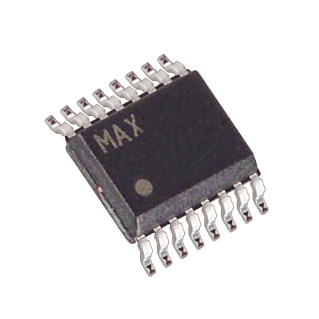
- Part No.:
- MAX3100CEE+
- Manufacturer:
- Analog Devices Inc./Maxim Integrated
- Category:
- Controllers
- Package:
- 16-SSOP (0.154", 3.90mm Width)
- Datasheet:
-
 MAX3100CEE+.pdf
- Description:
- IC UART SPI/MICRWIRE COMP 16QSOP
- Quantity:
- Payment:

- Shipping:

Inventory:3,199
Please send an inquiry. Send us your inquiry, and we will respond immediately.
Product details
Overview
MAX3100CEE+ from Maxim Integrated is a SPI/MICROWIRE-compatible universal asynchronous receiver-transmitter (UART) optimized for microcontroller-based systems. It integrates a crystal oscillator, 8-word FIFO, IrDA timing mode, and hardware/software shutdown - delivering up to 230 kbaud with 3.6864 MHz crystal, 150 µA operating current at 3.3 V, and 10 µA shutdown current. It enables isolated RS-232/RS-485 links and low-cost IR data communication in compact QSOP-16 packaging.
For engineers reviewing the MAX3100CEE+ datasheet, MAX3100CEE+ pinout, MAX3100CEE+ application, or MAX3100CEE+ equivalent, this page provides verified technical context, real-world interface constraints (e.g., Schmitt-trigger inputs, 25 mA TX/RTS sink capability), exact FIFO behavior under high-data-rate loads, IrDA SIR timing compliance, and validated alternatives for UART-in-SPI system upgrades.
Technical Context
The MAX3100CEE+ implements a full UART core with configurable 7-/8-bit word length, parity enable/disable, and 1–2 stop bits, all programmable via 16-bit SPI writes. Its baud-rate generator uses B0–B3 bits to select 16 division ratios, supporting standard rates from 300 to 230 kbaud with 1.8432 MHz or 3.6864 MHz crystals.
It features dual interrupt sources - receive activity detection during shutdown (RA bit) and framing error (FE bit) in normal operation - both maskable via RAM register. The IRQ output is open-drain, compatible with 5 V tolerant µC inputs, and cleared on Read Data operation.
Key Specifications
| Parameter | Value and Actual Design Meaning |
|---|---|
| Interface | SPI/MICROWIRE-compatible synchronous serial; 16-bit word protocol with CS-controlled framing |
| Max Baud Rate | 230 kbaud with 3.6864 MHz crystal; supports IrDA SIR timing mode |
| FIFO Depth | 8-word deep receive FIFO; reduces µC polling overhead at high data rates |
| Supply Voltage | +2.7 V to +5.5 V; operates across industrial and commercial voltage rails |
| Shutdown Current | 10 µA at TA = +25°C; maintains RX activity detection while minimizing power |
| TX/RTS Drive | Sinks 25 mA at VCC = 3.3 V; directly drives opto-coupler LEDs without external buffers |
| Input Thresholds | Schmitt-trigger inputs on DIN, SCLK, CS, SHDN, CTS, RX; improves noise immunity in noisy environments |
Pinout & Package
MAX3100CEE+ is housed in a 16-pin QSOP package (5.3 mm × 10.2 mm, 1.0 mm height) with lead-free/RoHS-compliant finish. Pin 1 is marked by a dot; pin numbering follows standard counter-clockwise orientation from top-left corner.
| Pin/Terminal | Circuit Role | Design Meaning |
|---|---|---|
| DIN (Pin 1) | SPI serial data input | Schmitt-triggered; latched on SCLK rising edge; initiates 16-bit command decode |
| DOUT (Pin 2) | SPI serial data output | High-impedance when CS = high; outputs read-config/read-data words |
| SCLK (Pin 3) | SPI clock input | Schmitt-triggered; falling-edge DOUT valid; rising-edge DIN sampled |
| CS (Pin 4) | Active-low chip select | Enables SPI interface; rising edge commits configuration/data writes |
| GND (Pin 8) | Ground reference | Primary analog/digital return; connects to PCB ground plane |
| X1 (Pin 10) | Clock input / crystal terminal | Accepts 1.8432 MHz or 3.6864 MHz crystal; also accepts external square-wave clock |
| X2 (Pin 9) | Clock output / crystal terminal | Connects to crystal second terminal; leave unconnected for external clock mode |
| RX (Pin 14) | Asynchronous receive input | High-to-low start-bit detection; majority-sampled at 16× baud rate |
| TX (Pin 15) | Asynchronous transmit output | Drives RS-232/RS-485 transceivers or opto-couplers directly (25 mA sink) |
| VCC (Pin 16) | Positive supply | +2.7 V to +5.5 V; powers internal logic, oscillator, and I/O drivers |
| IRQ (Pin 6) | Open-drain interrupt output | Asserted low on R, T, PM, or RA/FE events; requires external pull-up |
| SHDN (Pin 7) | Hardware shutdown control | Logic-low forces immediate oscillator stop and 10 µA shutdown current |
| CTS (Pin 11) | Clear-to-send input | General-purpose active-low input; readable via status register; used for flow control |
| RTS (Pin 13) | Request-to-send output | Active-low general-purpose output; software-controllable; drives RS-485 DE pin |
Key Features
| Feature | Design Value |
|---|---|
| IrDA SIR timing mode | Configurable via IR bit; enables 3/16-wide pulse widths for infrared data association compliance |
| 9-bit address recognition | Interrupt generated on matching 9-bit address frame; supports multi-drop networks without µC polling |
| Receive activity interrupt in shutdown | RA bit asserts IRQ on RX transition during 10 µA shutdown; enables wake-on-RX functionality |
| Opto-coupler direct drive | TX and RTS sink 25 mA at VCC = 3.3 V; eliminates need for external transistor buffers in isolated interfaces |
| Flexible interrupt masking | Four independent mask bits (RM, TM, PM, RAM) allow selective IRQ assertion per event source |
| Crystal oscillator integration | On-chip oscillator supports 1.8432 MHz or 3.6864 MHz crystals; eliminates external clock generator IC |
Applications
| Handheld Instruments | Intelligent Instrumentation |
|---|---|
Use Scenario: Battery-powered handheld test meters requiring low-power serial telemetry to host PC or cloud gateway. IC Role / Device Role / Timing Role: UART bridge between ARM Cortex-M0+ MCU and isolated RS-232/USB-UART adapter; manages IrDA link to legacy PDAs. Use Value: 10 µA shutdown current extends battery life; 8-word FIFO prevents data loss during µC sleep cycles; Schmitt-trigger inputs reject EMI in field environments. |
Use Scenario: Programmable logic controller (PLC) I/O modules with embedded diagnostics and remote firmware update over RS-485. IC Role / Device Role / Timing Role: SPI-to-asynchronous bridge enabling µC to communicate with Modbus RTU slave devices; handles 9-bit address frames for node selection. Use Value: Hardware RTS control synchronizes RS-485 driver enable; 230 kbaud supports high-speed firmware upload; IrDA mode enables wireless commissioning. |
| UART in SPI Systems | Isolated RS-232/RS-485 |
Use Scenario: Resource-constrained IoT edge nodes using SPI-only MCUs (e.g., STM32L0) needing UART peripherals for sensor aggregation. IC Role / Device Role / Timing Role: Offloads UART protocol handling from µC; provides configurable parity, stop bits, and FIFO management via SPI registers. Use Value: Reduces µC firmware size and CPU load; eliminates need for external UART with parallel bus; SPI interface simplifies PCB routing. |
Use Scenario: Medical device isolation barrier where patient-connected circuits require galvanic separation from host MCU. IC Role / Device Role / Timing Role: Drives opto-couplers directly on TX/RTS lines; receives opto-isolated RX signals via Schmitt-trigger inputs. Use Value: 25 mA TX sink drives 6N136 LED directly; no external buffer needed; 1.8432 MHz crystal ensures <1% baud error for reliable Modbus communication. |
Equivalent & Alternatives
The following parts are listed as comparable options for similar UART bridging applications.
| Alternative Part | Technical Difference | Application Difference | Selection Advice |
|---|---|---|---|
| MAX3107EEE+ | 32-word FIFO, integrated ±15 kV ESD protection, 3.3 V only, TQFN-24 package | Better suited for high-noise industrial RS-232 ports; lacks hardware SHDN pin | Select when ESD robustness and deeper FIFO are required; not drop-in due to different pin count and voltage range |
| SC16IS752IPW | I²C/SPI dual-interface, 64-byte FIFO, programmable GPIOs, 2.5–5.5 V operation, TSSOP-28 | Supports I²C master systems; includes auxiliary GPIOs for modem control signaling | Choose for mixed-bus designs or when additional GPIOs simplify system-level handshaking |
Compared with MAX3100CEE+, MAX3107EEE+ offers higher ESD tolerance and larger FIFO but sacrifices hardware shutdown and wide-voltage flexibility; SC16IS752IPW adds I²C support and GPIOs at the cost of larger footprint and non-QSOP packaging - making MAX3100CEE+ optimal for space-constrained, low-power SPI-only microcontroller interfaces.
Availability
MAX3100CEE+ is available at Aetrix Electronics and suitable for handheld instruments, intelligent instrumentation, UART-in-SPI systems, isolated RS-232/RS-485 interfaces, and low-cost IR data links requiring stable component supply across commercial temperature range (0°C to +70°C).
Supply support for MAX3100CEE+ includes scheduled delivery planning, volume procurement assistance, BOM continuity management, traceable sourcing, and lifecycle availability coordination for OEM customers, industrial embedded developers, connected-device designers, and electronics production programs.
Manufacturer
Maxim Integrated (now part of Analog Devices) is a semiconductor design house specializing in precision analog, mixed-signal, and high-reliability interface solutions for industrial, medical, and communications markets.
The MAX3100 product line was designed specifically to embed UART functionality into SPI-based microcontroller systems - eliminating parallel-bus UARTs and reducing µC pin count, PCB area, and firmware complexity in space- and power-sensitive applications.
FAQ
What is the maximum crystal frequency supported by the MAX3100CEE+?
The MAX3100CEE+ supports 1.8432 MHz and 3.6864 MHz crystals as specified in the datasheet. While X1 can accept an external square-wave clock up to 23.04 MHz (for 230.4 kbaud ÷ 16), the internal oscillator circuitry is characterized only for those two crystal frequencies. Using other crystals may result in baud-rate inaccuracy exceeding 1%, risking communication failure with standard UART peripherals.
Does the MAX3100CEE+ support true hardware flow control with RTS/CTS?
Yes, the MAX3100CEE+ supports hardware flow control: RTS is a software-controllable active-low output that can drive RS-485 driver-enable pins, and CTS is a dedicated active-low input monitored by the µC via register reads. However, automatic RTS toggling based on FIFO level is not implemented - RTS state must be managed explicitly by firmware to assert before transmission and deassert after completion.
Can the MAX3100CEE+ operate with a 5 V supply while interfacing to a 3.3 V microcontroller SPI bus?
Yes - the MAX3100CEE+ accepts VCC from +2.7 V to +5.5 V, and its SPI inputs (DIN, SCLK, CS, SHDN, CTS) have VIH = 0.7 × VCC and VIL = 0.3 × VCC. At VCC = 5 V, VIH = 3.5 V, so a 3.3 V µC's logic-high output (typically ≥3.0 V) may fall below guaranteed recognition threshold. Use level-shifting or ensure µC IO is 5 V tolerant; alternatively, operate MAX3100CEE+ at 3.3 V for guaranteed compatibility.
How does the MAX3100CEE+ handle framing errors during shutdown mode?
In shutdown mode, the RA/FE register bit functions exclusively as Receive Activity (RA), not Framing Error (FE). A transition on RX sets RA = 1 and asserts IRQ if RAM = 1 - enabling wake-on-RX. FE detection is disabled during shutdown. Upon exit from shutdown, the first received character may cause a framing error due to oscillator startup delay; this FE bit is cleared automatically upon receipt of the next properly framed character.
Is the MAX3100CEE+ pinout compatible with other MAX3100 variants like MAX3100CPD+?
No - the MAX3100CEE+ (QSOP-16) and MAX3100CPD+ (14-pin DIP) have different pin counts and incompatible pin mappings. For example, IRQ is on Pin 6 in QSOP but Pin 14 in DIP; X1/X2 positions differ; and DIP includes N.C. pins absent in QSOP. Board redesign is required when switching packages - refer to Pin Configurations section of datasheet Rev 2 for exact mapping per variant.
MAX3100CEE+ Specifications
- Product attributes
- Attribute value
- Manufacturer:
- Analog Devices Inc./Maxim Integrated
- Package/Case:
- 16-SSOP (0.154", 3.90mm Width)
- Programmable:
- Not Verified
- Protocol:
- RS232, RS485
- Function:
- Controller
- Interface:
- SPI, UART
- Standards:
- -
- Voltage - Supply:
- 2.7V ~ 5.5V
- Current - Supply:
- 150µA
- Operating Temperature:
- 0°C ~ 70°C
- Supplier Device Package:
- 16-QSOP
- Grade:
- -
- Qualification:
- -
MAX3100CEE+ FAQ
1.How can I place an order for MAX3100CEE+ through Aetrix?
Please submit a Request for Quotation (RFQ) for MAX3100CEE+ on Aetrix. Our sales agent will provide a competitive quotation and guide you through the order confirmation once you accept the terms.
2.Are the price and stock information for MAX3100CEE+ reliable?
The price and inventory of MAX3100CEE+ are updated periodically and may fluctuate due to market conditions. Stock and pricing data are typically refreshed every 24 hours. Quotation validity for MAX3100CEE+ is usually 5 days.
3.What payment methods are accepted for MAX3100CEE+?
We accept Wire Transfer, PayPal, Credit Card, Western Union, MoneyGram, and Escrow for MAX3100CEE+ transactions.
Note: Certain payment methods may incur a processing fee.
4.How is shipping managed for MAX3100CEE+?
MAX3100CEE+ orders can be shipped via leading logistics carriers, including DHL, UPS, FedEx, TNT, or Registered Mail.
Once your MAX3100CEE+ order is processed, you will receive an email with the shipment details and tracking number.
Note: Tracking information may take up to 24 hours to appear. Express delivery typically takes 3–5 business days.
5.How can I obtain technical support or documentation for MAX3100CEE+?
For technical support, including MAX3100CEE+ datasheets, pinout diagrams, or application guidance, please contact our engineering support team. They can provide detailed documentation and assistance for your MAX3100CEE+ requirements.
6.How does Aetrix verify that MAX3100CEE+ is sourced from the original manufacturer or authorized distributors?
All MAX3100CEE+ products on Aetrix are procured from qualified distributors and authorized channels. Our dedicated quality assurance team conducts strict verification, including traceability checks and, if necessary, third-party testing. This ensures that MAX3100CEE+ meets industry standards.
7.What is the process for return or replacement of MAX3100CEE+?
All MAX3100CEE+ units undergo pre-shipment inspection (PSI). If there is an issue with MAX3100CEE+, returns or replacements are accepted under the following conditions:
1.Quantity discrepancies, incorrect items, or visible external defects (such as breakage or corrosion), acknowledged by Aetrix.
2.The issue is reported within 90 days of delivery.
3.The MAX3100CEE+ part is unused and in its original packaging.
Return procedure for MAX3100CEE+:
1.Submit a request within 90 days.
2.Obtain a Return Material Authorization (RMA) from Aetrix.
MAX3100CEE+ Tags

-
PTN5150AHXMP
NXP Semiconductors

-
USB3740B-AI9-TR
Microchip Technology

-
USB3740B-AI2-TR
Microchip Technology

-
USB3300-EZK-TR
Microchip Technology
-
USB3300-EZK
Microchip Technology

-
FUSB340TMX
onsemi

-
FUSB302BMPX
onsemi

-
DP83826IRHBR
Texas Instruments

-
MCP2518FDT-E/QBB
Microchip Technology
-
FUSB302MPX
onsemi

-
MCP2518FDT-E/SL
Microchip Technology

-
FT260Q-R
FTDI, Future Technology Devices International Ltd
Tech Hub

A practical engineering guide to 3.3V and 5V logic compatibility, input thresholds, resistor dividers, translator ICs, MOSFET level shifting, I2C pull-ups, timing limits and power-sequencing risks.

The 74HC595 uses push-pull logic outputs, while the TPIC6B595 uses 50 V open-drain DMOS sinks for higher-power loads. This guide compares timing, current limits, 3.3 V interfacing, load wiring, thermal…

The 74HC595 converts serial data into eight stable parallel outputs. This guide covers pin functions, shift and storage timing, OE and MR behavior, drive-current limits, cascading, voltage compatibilit…

A technical comparison of level-sensitive latches and edge-triggered flip-flops, covering timing windows, setup and hold limits, master–slave operation, time borrowing, race-through, HDL inference and…

A D latch stores one bit while Enable controls when data can pass. This reference covers gate-level operation, truth tables, transparency, setup and hold timing, LE versus OE, common ICs and practical …

An SR latch stores one bit through cross-coupled feedback. This engineering reference covers NOR and NAND implementations, truth tables, forbidden-state recovery, gated operation, switch debouncing, fa…

Latch circuits retain one bit through feedback. This technical reference covers SR and D latches, truth tables, transparency, timing limits, latch-versus-flip-flop behavior, applications and common log…

An engineering guide to LED driver operation, constant-current and constant-voltage outputs, linear and switching topologies, dimming, IC selection, calculations, replacement compatibility, and fault c…

Operational amplifier guide covering op amp basics, feedback, ideal vs real op amps, common configurations, buffer circuits, offset, bias current, gain-bandwidth, slew rate, rail-to-rail limits and sel…

Jumper cables guide covering safe connection order, red and black clamp placement, final ground connection, cable gauge, length, clamp quality, copper vs CCA cables, jump starter comparison and battery…


