
 My Inquiry
 My Account


Analog Devices Inc./Maxim Integrated MAX31850JATB+T
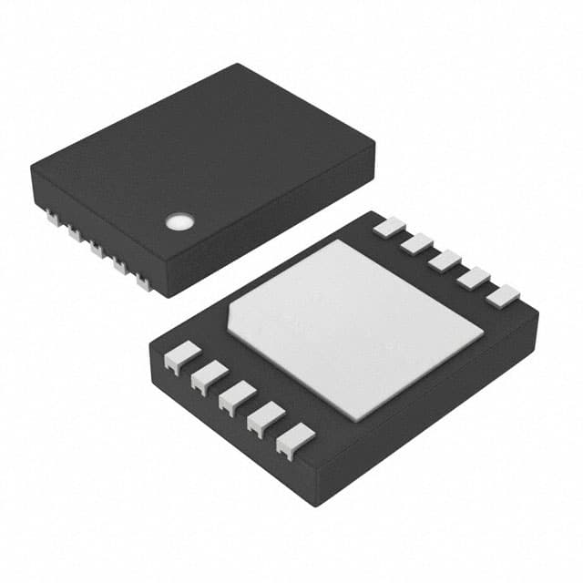
- Part No.:
- MAX31850JATB+T
- Manufacturer:
- Analog Devices Inc./Maxim Integrated
- Category:
- Sensor and Detector Interfaces
- Package:
- 10-WFDFN Exposed Pad
- Datasheet:
-
 MAX31850JATB+T.pdf
- Description:
- IC CONV THRMCPLE-DIG J TYPE TDFN
- Quantity:
- Payment:

- Shipping:

Inventory:3,151
Please send an inquiry. Send us your inquiry, and we will respond immediately.
Product details
Overview
MAX31850JATB+T from Maxim Integrated is a cold-junction compensated, 1-Wire thermocouple-to-digital converter optimized for J-type thermocouples. It delivers 14-bit resolution (0.25°C), supports -210°C to +1200°C thermocouple range, achieves ±2°C accuracy from -210°C to +750°C, and operates from -40°C to +125°C ambient. It enables distributed temperature monitoring in industrial process control systems using parasitic or local power.
For engineers reviewing the MAX31850JATB+T datasheet, MAX31850JATB+T pinout, MAX31850JATB+T application, or MAX31850JATB+T equivalent, key selection considerations include J-type thermocouple support, 1-Wire multdrop capability, integrated cold-junction compensation, fault detection (open/short), and TDFN-EP package compatibility with space-constrained PCB layouts.
Technical Context
The MAX31850JATB+T integrates a precision 14-bit ADC, internal cold-junction temperature sensor, digital controller, and 1-Wire interface logic. Its signal path includes dedicated thermocouple input conditioning (T+/T−), programmable location address inputs (AD0–AD3), and fault-detection circuitry that identifies open circuits and shorts to VDD or GND.
It performs three synchronized operations during each conversion cycle: cold-junction temperature measurement, thermocouple voltage digitization, and real-time fault checking-all within a guaranteed 72–100ms conversion time. The device uses linear gain compensation (57.953 µV/°C nominal) calibrated specifically for J-type thermocouples, and stores results in a defined scratchpad memory map with CRC-protected data integrity.
Key Specifications
| Parameter | Value and Actual Design Meaning |
|---|---|
| Thermocouple Type | J-type only - hardware-trimmed analog front-end and gain calibration ensure accurate linearized output without external correction tables. |
| Temperature Resolution | 0.25°C - 14-bit output format enables fine-grained thermal trending and closed-loop control stability. |
| Accuracy (Thermocouple) | ±2°C over -210°C to +750°C - specified error bound includes gain/offset drift and cold-junction compensation error, usable for Class 1 industrial sensing. |
| Conversion Time | 72–100 ms - fixed-duration cycle covering cold-junction read, thermocouple digitization, and fault detection; determines minimum polling interval. |
| Operating Voltage | 3.0–3.7 V - supports both local VDD supply and parasite power via DQ; requires strong pullup during conversion in parasite mode. |
| Ambient Range | -40°C to +125°C - qualified for harsh environments including motor drives, HVAC ducts, and industrial enclosures. |
| Fault Detection | Open thermocouple, short-to-GND, short-to-VDD - status bits embedded in scratchpad byte 2/3 enable immediate system-level error response. |
Pinout & Package
TDFN-EP (3mm × 4mm, 10-pin, exposed pad). Pin 10 (DNC) must remain unconnected; EP may be grounded or left floating per layout requirements.
| Pin/Terminal | Circuit Role | Design Meaning |
|---|---|---|
| GND (Pin 1) | Reference ground | Primary return path for thermocouple signals, internal circuitry, and parasite-power capacitor discharge. |
| T− (Pin 2) | Thermocouple negative input | Connected to Constantan wire; internally biased at ~0.5×VDD to reject common-mode noise on long leads. |
| T+ (Pin 3) | Thermocouple positive input | Connected to Iron wire; differential pair with T− feeds dedicated instrumentation amplifier stage. |
| VDD (Pin 4) | Power supply input | Required for local power mode; must be tied to GND in parasite-power configuration. |
| DQ (Pin 5) | 1-Wire bidirectional I/O | Open-drain interface carrying command/data and parasitic power; requires external 4.7kΩ pullup. |
| AD0–AD3 (Pins 6–9) | Location address inputs | Hardwired LSB→MSB address bits; read back in config register to identify physical sensor location in multi-node systems. |
Key Features
| Feature | Design Value |
|---|---|
| Integrated cold-junction compensation | On-die temperature sensor with ±2°C error (−40°C to +100°C) eliminates need for external RTD or thermistor reference. |
| 1-Wire multdrop architecture | Single bus supports >100 devices via unique 64-bit ROM IDs - reduces wiring complexity and microcontroller GPIO count in distributed sensing. |
| J-type thermocouple optimization | Factory-trimmed 57.953 µV/°C gain and offset - avoids software linearization overhead and improves repeatability vs generic converters. |
| Real-time fault diagnostics | Dedicated hardware detects open thermocouple, short-to-GND, and short-to-VDD - status flags enable fail-safe shutdown before thermal runaway. |
| Parasite-power capability | Operates with no local VDD - ideal for sealed probes, rotating machinery sensors, or retrofit installations where power routing is impractical. |
Applications
| Industrial Process Monitoring | HVAC System Control |
|---|---|
Use Scenario: Continuous temperature logging of reactor vessels, steam lines, and extruder barrels in chemical plants. IC Role / Device Role / Timing Role: Primary thermocouple digitizer with cold-junction compensation, delivering calibrated J-type readings every 100ms over daisy-chained 1-Wire bus. Use Value: Enables centralized SCADA integration without per-sensor signal conditioners; fault flags prevent false alarms from broken thermocouple wires. | Use Scenario: Zoned air temperature feedback in commercial HVAC units with multiple duct-mounted probes. IC Role / Device Role / Timing Role: Local sensor node converting J-type thermocouple output to digital data for microcontroller-based PID loop execution. Use Value: Reduces BOM cost by eliminating separate ADCs and reference ICs; AD0–AD3 pins allow firmware to map physical duct locations without EEPROM programming. |
| Appliance Thermal Safety | Medical Equipment Calibration |
Use Scenario: Overtemperature cutoff in induction cooktops and commercial ovens using embedded J-type sensors. IC Role / Device Role / Timing Role: Safety-critical temperature monitor interfacing directly to appliance MCU via 1-Wire, with open-circuit detection preventing silent failure. Use Value: Meets IEC 60730 Class B requirements through hardware fault reporting; parasitic power simplifies sensor module design in high-voltage isolation zones. | Use Scenario: Reference-grade temperature verification in portable diagnostic devices requiring traceable thermal calibration. IC Role / Device Role / Timing Role: High-accuracy J-type interface providing 0.25°C resolution data to embedded ARM processor for real-time thermal drift compensation. Use Value: ±2°C accuracy over -210°C to +750°C meets ASTM E230 Grade 1 tolerance; internal cold-junction sensor removes external reference uncertainty. |
Equivalent & Alternatives
The following parts are listed as comparable options for similar thermocouple-to-digital conversion applications.
| Alternative Part | Technical Difference | Application Difference | Selection Advice |
|---|---|---|---|
| MAX31855KASA+ | Supports K-type only; SPI interface; no 1-Wire; higher quiescent current (1.5mA active); same TDFN package. | Requires dedicated SPI lines and MCU GPIOs; better suited for single-sensor, high-speed acquisition vs. large-scale distributed networks. | Select when SPI infrastructure exists and J-type compatibility is not required. |
| AD8495ARZ | Analog output (10mV/°C); no digitization or cold-junction compensation; requires external ADC and microcontroller. | Demands additional signal chain components; lacks built-in fault detection and 1-Wire addressing. | Select for analog-only systems or where existing ADC resources are available and board space permits added components. |
Compared with MAX31855KASA+, MAX31850JATB+T reduces wiring and MCU resource load via 1-Wire multdrop but trades off SPI speed and K-type flexibility. Against AD8495ARZ, it delivers full turnkey digital output with integrated diagnostics-eliminating design risk from external component tolerances and layout sensitivity.
Availability
MAX31850JATB+T is available at Aetrix Electronics and suitable for industrial process monitoring, HVAC system control, and appliance thermal safety requiring stable component supply across extended production lifecycles.
Supply support for MAX31850JATB+T includes scheduled delivery planning, volume procurement assistance, BOM continuity management, traceable sourcing, and lifecycle availability coordination for OEM customers, industrial embedded developers, connected-device designers, and electronics production programs.
Manufacturer
Maxim Integrated (now part of Analog Devices) designs precision analog and mixed-signal ICs for demanding industrial, medical, and communications applications.
The MAX31850 product line delivers integrated thermocouple interface solutions with embedded cold-junction compensation and 1-Wire connectivity-targeting distributed, low-wiring-cost temperature sensing in harsh environments.
FAQ
What thermocouple types does the MAX31850JATB+T support?
The MAX31850JATB+T is factory trimmed and calibrated exclusively for J-type thermocouples. Its analog front-end, gain coefficient (57.953 µV/°C), and internal compensation algorithms are optimized for J-type characteristics. It does not support K-, N-, T-, E-, R-, or S-type thermocouples - those require other variants such as MAX31850KATB+T or MAX31851SATB+T. Using a non-J thermocouple with MAX31850JATB+T will produce inaccurate readings.
Does the MAX31850JATB+T require an external power supply?
No - the MAX31850JATB+T supports parasite power via the DQ pin, eliminating the need for a local VDD supply. In parasite mode, VDD must be connected to GND, and a strong pullup (e.g., MOSFET-switched rail) is required during temperature conversions to sustain 1.5mA peak current. For continuous operation above +100°C or high-reliability applications, local VDD supply is recommended to avoid leakage-related communication failures.
How does the MAX31850JATB+T detect thermocouple faults?
The MAX31850JATB+T performs autonomous fault detection during every conversion cycle. It checks for open thermocouples and shorts to GND or VDD on the T+ and T− inputs using dedicated internal circuitry. Fault status is encoded in bits 0–2 of scratchpad byte 2: bit 0 = open circuit, bit 1 = short to GND, bit 2 = short to VDD. These flags appear alongside temperature data, enabling immediate system-level response without additional external components.
What is the purpose of the AD0–AD3 pins on the MAX31850JATB+T?
The AD0–AD3 pins on the MAX31850JATB+T provide hardware-programmable location addressing. Each pin can be tied to GND (logic 0) or DQ (logic 1) to assign a unique 4-bit address (0000–1111), allowing up to 16 physically distinct sensors to be mapped on the same 1-Wire bus. Their programmed values are readable in bits [3:0] of scratchpad byte 4, enabling firmware to correlate raw 64-bit ROM IDs with physical installation points without external EEPROM or manual configuration.
What is the maximum operating temperature range for the MAX31850JATB+T?
The MAX31850JATB+T is rated for an ambient operating temperature range of -40°C to +125°C. This specification applies to the IC's junction and package environment. While the J-type thermocouple itself supports up to +1200°C at the hot junction, the MAX31850JATB+T's accuracy and reliability are guaranteed only within its specified ambient range. Operation beyond +125°C ambient may cause parametric shift or communication failure, especially in parasite-power mode.
MAX31850JATB+T Specifications
- Product attributes
- Attribute value
- Manufacturer:
- Analog Devices Inc./Maxim Integrated
- Package/Case:
- 10-WFDFN Exposed Pad
- Series:
- -
- Packaging:
- Tape & Reel (TR)
- Product Status:
- Active
- Programmable:
- Not Verified
- Type:
- Thermocouple to Digital Converter
- Input Type:
- Thermocouple (Multiple)
- Output Type:
- Digital
- Current - Supply:
- 900 µA
- Operating Temperature:
- -40°C ~ 125°C
- Grade:
- -
- Qualification:
- -
- Mounting Type:
- Surface Mount
- Supplier Device Package:
- 10-TDFN (3x4)
MAX31850JATB+T FAQ
1.How can I place an order for MAX31850JATB+T through Aetrix?
Please submit a Request for Quotation (RFQ) for MAX31850JATB+T on Aetrix. Our sales agent will provide a competitive quotation and guide you through the order confirmation once you accept the terms.
2.Are the price and stock information for MAX31850JATB+T reliable?
The price and inventory of MAX31850JATB+T are updated periodically and may fluctuate due to market conditions. Stock and pricing data are typically refreshed every 24 hours. Quotation validity for MAX31850JATB+T is usually 5 days.
3.What payment methods are accepted for MAX31850JATB+T?
We accept Wire Transfer, PayPal, Credit Card, Western Union, MoneyGram, and Escrow for MAX31850JATB+T transactions.
Note: Certain payment methods may incur a processing fee.
4.How is shipping managed for MAX31850JATB+T?
MAX31850JATB+T orders can be shipped via leading logistics carriers, including DHL, UPS, FedEx, TNT, or Registered Mail.
Once your MAX31850JATB+T order is processed, you will receive an email with the shipment details and tracking number.
Note: Tracking information may take up to 24 hours to appear. Express delivery typically takes 3–5 business days.
5.How can I obtain technical support or documentation for MAX31850JATB+T?
For technical support, including MAX31850JATB+T datasheets, pinout diagrams, or application guidance, please contact our engineering support team. They can provide detailed documentation and assistance for your MAX31850JATB+T requirements.
6.How does Aetrix verify that MAX31850JATB+T is sourced from the original manufacturer or authorized distributors?
All MAX31850JATB+T products on Aetrix are procured from qualified distributors and authorized channels. Our dedicated quality assurance team conducts strict verification, including traceability checks and, if necessary, third-party testing. This ensures that MAX31850JATB+T meets industry standards.
7.What is the process for return or replacement of MAX31850JATB+T?
All MAX31850JATB+T units undergo pre-shipment inspection (PSI). If there is an issue with MAX31850JATB+T, returns or replacements are accepted under the following conditions:
1.Quantity discrepancies, incorrect items, or visible external defects (such as breakage or corrosion), acknowledged by Aetrix.
2.The issue is reported within 90 days of delivery.
3.The MAX31850JATB+T part is unused and in its original packaging.
Return procedure for MAX31850JATB+T:
1.Submit a request within 90 days.
2.Obtain a Return Material Authorization (RMA) from Aetrix.
MAX31850JATB+T Tags

-
RE46C100S8TF
Microchip Technology

-
XTR111AIDRCR
Texas Instruments

-
XTR111AIDGQR
Texas Instruments

-
XTR117AIDGKR
Texas Instruments
-
XTR111AIDGQT
Texas Instruments

-
XTR115UA/2K5
Texas Instruments
-
MAX14626ETT+T
Analog Devices Inc./Maxim Integrated
-
XTR116UA/2K5
Texas Instruments
-
XTR115U/2K5
Texas Instruments
-
XTR116U/2K5
Texas Instruments

-
PGA308AIDGSR
Texas Instruments
-
XTR300AIRGWR
Texas Instruments
Tech Hub

A practical engineering guide to 3.3V and 5V logic compatibility, input thresholds, resistor dividers, translator ICs, MOSFET level shifting, I2C pull-ups, timing limits and power-sequencing risks.

The 74HC595 uses push-pull logic outputs, while the TPIC6B595 uses 50 V open-drain DMOS sinks for higher-power loads. This guide compares timing, current limits, 3.3 V interfacing, load wiring, thermal…

The 74HC595 converts serial data into eight stable parallel outputs. This guide covers pin functions, shift and storage timing, OE and MR behavior, drive-current limits, cascading, voltage compatibilit…

A technical comparison of level-sensitive latches and edge-triggered flip-flops, covering timing windows, setup and hold limits, master–slave operation, time borrowing, race-through, HDL inference and…

A D latch stores one bit while Enable controls when data can pass. This reference covers gate-level operation, truth tables, transparency, setup and hold timing, LE versus OE, common ICs and practical …

An SR latch stores one bit through cross-coupled feedback. This engineering reference covers NOR and NAND implementations, truth tables, forbidden-state recovery, gated operation, switch debouncing, fa…

Latch circuits retain one bit through feedback. This technical reference covers SR and D latches, truth tables, transparency, timing limits, latch-versus-flip-flop behavior, applications and common log…

An engineering guide to LED driver operation, constant-current and constant-voltage outputs, linear and switching topologies, dimming, IC selection, calculations, replacement compatibility, and fault c…

Operational amplifier guide covering op amp basics, feedback, ideal vs real op amps, common configurations, buffer circuits, offset, bias current, gain-bandwidth, slew rate, rail-to-rail limits and sel…

Jumper cables guide covering safe connection order, red and black clamp placement, final ground connection, cable gauge, length, clamp quality, copper vs CCA cables, jump starter comparison and battery…


