
 My Inquiry
 My Account


Analog Devices Inc./Maxim Integrated MAX32625IWY+
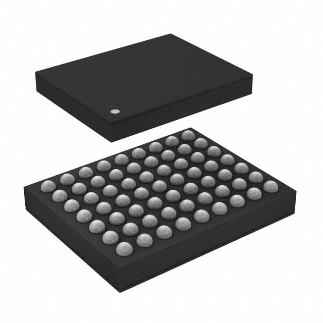
- Part No.:
- MAX32625IWY+
- Manufacturer:
- Analog Devices Inc./Maxim Integrated
- Category:
- Microcontrollers
- Package:
- 63-WFBGA, WLBGA
- Datasheet:
-
 MAX32625IWY+.pdf
- Description:
- IC MCU 32BIT 512KB FLASH 63WLP
- Quantity:
- Payment:

- Shipping:

Inventory:2,051
Please send an inquiry. Send us your inquiry, and we will respond immediately.
Product details
Overview
MAX32625IWY+ from Maxim Integrated is an ultra-low-power Arm® Cortex®-M4 with FPU microcontroller designed for wearable and IoT edge nodes. It delivers 96MHz peak performance, 512KB flash, 160KB SRAM, and operates from 1.2V core/1.8–3.3V I/O supplies. Its LP1 sleep mode draws just 2.56μW with 5μs wake-up-enabling multi-year battery life in fitness monitors and medical patches.
For engineers reviewing the MAX32625IWY+ datasheet, MAX32625IWY+ pinout, MAX32625IWY+ application, or MAX32625IWY+ equivalent, key selection criteria include its dual-clock architecture (96MHz/4MHz), hardware AES-128/192/256 engine, 10-bit delta-sigma ADC at 7.8ksps, and support for USB 2.0 full-speed device operation with integrated transceiver.
Technical Context
The MAX32625IWY+ implements a tightly coupled Arm Cortex-M4 core with floating-point unit and 8KB instruction cache, enabling efficient signal processing for sensor fusion and real-time biometric analysis. Its power management unit (PMU) supports four low-power modes-including LP0 (600nA with RTC) and LP1 (2.56μW data retention)-with dynamic clock gating and voltage scaling per subsystem.
Peripherals include three SPI masters (one supporting Execute-in-Place), two I²C masters, three UARTs, 1-Wire master, full-speed USB 2.0 device controller with internal PHY, sixteen PWM engines, six 32-bit timers, and a 10-bit delta-sigma ADC with selectable references and up to 5.5V input tolerance on AIN0/AIN1.
Key Specifications
| Parameter | Value and Actual Design Meaning |
|---|---|
| CPU Core | Arm Cortex-M4 with FPU and 8KB instruction cache for deterministic floating-point math in sensor algorithms. |
| Memory | 512KB flash (8KB page size, 10k erase cycles, 10-year data retention) and 160KB SRAM for firmware + buffer storage. |
| Power Modes | LP0: 600nA (RTC active); LP1: 2.56μW (full SRAM retention, 5μs wake-up); LP2: 27μA/MHz (deep sleep with peripheral clocks). |
| ADC | 10-bit delta-sigma with 7.8ksps sample rate, ±2 LSB INL, 58.5dB SNR, and 0.05–5.5V input range on AIN0/AIN1. |
| USB Interface | Full-speed USB 2.0 device with integrated transceiver, 3.3V ±5% VDDB supply, and compliance-ready 96MHz internal oscillator trimming. |
| Security | Hardware AES-128/-192/-256 engine; no TPU/MAA/PRNG (reserved for MAX32626 variant). |
| Operating Range | -30°C to +85°C ambient; 1.2V core (±5%), 1.8–3.3V I/O (individually configurable per pin group). |
Pinout & Package
MAX32625IWY+ is packaged in a 63-ball Wafer-Level Package (WLP), 3.3mm × 3.3mm, 0.4mm pitch, with 40 general-purpose I/O pins supporting multiple shared functions including SPI, I²C, UART, 1-Wire, USB DP/DM, and ADC inputs. The package is RoHS-compliant and optimized for ultra-thin wearable PCBs.
| Pin/Terminal | Circuit Role | Design Meaning |
|---|---|---|
| VDD12 | 1.2V Core Supply | Primary power for CPU, cache, and memory subsystems; regulated internally from VDDB or external source. |
| VDD18 | 1.8V Digital Supply | Supplies digital logic, PMU, and most peripherals; must be ≥1.71V for guaranteed operation. |
| VDDIO / VDDIOH | I/O Voltage Rails | VDDIO (1.71–3.6V) and VDDIOH (≥VDDIO) independently power GPIO banks for mixed-voltage interfacing. |
| AIN0–AIN3 | Analog Inputs | Dedicated delta-sigma ADC channels; AIN0/AIN1 tolerate up to 5.5V, enabling direct connection to high-voltage sensors. |
| DP / DM | USB Differential Pair | Integrated full-speed USB 2.0 transceiver signals; require no external termination or magnetics in device-only applications. |
| RSTN / SRSTN | Reset Inputs | Asynchronous active-low resets: RSTN monitored against VRTC, SRSTN against VDDIO for flexible system control. |
| TCK / TMS / TDI / TDO | JTAG/SWD Debug | Serial Wire Debug (SWD) interface compatible with standard ARM debug tools; supports programming and real-time trace. |
Key Features
| Feature | Design Value |
|---|---|
| Dual-frequency clock system | Factory-trimmed 96MHz oscillator for performance-critical tasks and 4MHz RC oscillator for always-on monitoring-no external crystal required. |
| SPI Execute-in-Place (SPIX) | Direct code execution from external SPI flash via dedicated SPIX engine, reducing SRAM footprint and enabling scalable firmware updates. |
| Configurable I/O voltage domains | Each GPIO bank powered by independent VDDIO or VDDIOH rails, allowing seamless interfacing with 1.8V, 2.5V, and 3.3V peripherals without level shifters. |
| Ultra-fast LP1 wake-up | 5μs transition from 2.56μW data-retention sleep to full 96MHz operation-critical for duty-cycled sensor sampling in battery-constrained wearables. |
| Robust analog front-end | 10-bit delta-sigma ADC with programmable gain, internal reference, and 5.5V-tolerant AIN0/AIN1 inputs-supports direct integration of thermistors, ECG electrodes, and strain gauges. |
Applications
| Sports Watches | Fitness Monitors |
|---|---|
Use Scenario: Continuous heart-rate, motion, and GPS logging during multi-hour athletic sessions with sub-10-second GPS acquisition. IC Role / Device Role / Timing Role: Central MCU managing sensor fusion, BLE connectivity, display refresh, and power-gated GPS module wake-up via RTC alarm. Use Value: LP2 mode (27μA/MHz) enables 2-week battery life; 96MHz burst processing handles FFT-based HRV analysis without external DSP. | Use Scenario: Real-time step counting, calorie estimation, and sleep-stage classification using accelerometer, gyroscope, and PPG data. IC Role / Device Role / Timing Role: Sensor hub aggregating asynchronous I²C/SPI sensor streams, running adaptive filtering algorithms, and transmitting compressed results over BLE. Use Value: 4MHz low-power clock sustains background activity; 10-bit ADC captures PPG waveform fidelity for SpO₂ estimation. |
| Wearable Medical Patches | Portable Medical Devices |
Use Scenario: 72-hour continuous ECG and temperature monitoring for arrhythmia detection in ambulatory patients. IC Role / Device Role / Timing Role: Biopotential acquisition controller with analog front-end biasing, digital notch filtering, and secure local storage before encrypted BLE transmission. Use Value: AIN0/AIN1 5.5V tolerance allows direct electrode connection; hardware AES encrypts stored ECG traces prior to upload. | Use Scenario: Handheld spirometers and glucose meters requiring FDA-grade accuracy, audit logging, and USB mass-storage firmware updates. IC Role / Device Role / Timing Role: Application processor executing calibrated sensor algorithms, managing user interface, and acting as USB MSC device for clinical data export. Use Value: Full-speed USB 2.0 with integrated PHY eliminates external components; 512KB flash stores calibration tables and regulatory audit logs. |
Equivalent & Alternatives
The following parts are listed as comparable options for similar microcontroller applications.
| Alternative Part | Technical Difference | Application Difference | Selection Advice |
|---|---|---|---|
| Nordic nRF52840-QIAA | Integrated Bluetooth 5.0 radio; lower flash (1MB) but no hardware AES acceleration; 64MHz Cortex-M4F; lacks 5.5V-tolerant ADC inputs. | Better suited for BLE-centric designs where RF stack offload is critical; less optimal for analog-intensive medical sensing without external signal conditioning. | Select when wireless connectivity dominates requirements and analog channel count/voltage range is secondary. |
| TI MSP432E401Y | 120MHz Cortex-M4F; 1MB flash/256KB SRAM; 12-bit SAR ADC (1MSPS); no integrated USB PHY; requires external crystal for USB compliance. | Higher performance for motor control or industrial HMI; larger footprint (TQFP-100); higher active current (120μA/MHz) limits wearable runtime. | Prefer for applications needing >96MHz deterministic throughput or 12-bit ADC speed, accepting trade-offs in power and package size. |
Compared with nRF52840-QIAA and MSP432E401Y, the MAX32625IWY+ uniquely balances ultra-low-power sleep states (600nA LP0), 5.5V-tolerant analog inputs, and integrated USB PHY in a 3.3mm WLP-making it optimal for compact, battery-powered medical and sports wearables demanding analog fidelity and long runtime.
Availability
MAX32625IWY+ is available at Aetrix Electronics and suitable for sports watches, fitness monitors, and wearable medical patches requiring stable component supply across multi-year production lifecycles.
Supply support for MAX32625IWY+ includes scheduled delivery planning, volume procurement assistance, BOM continuity management, traceable sourcing, and lifecycle availability coordination for OEM customers, industrial embedded developers, connected-device designers, and electronics production programs.
Manufacturer
Maxim Integrated, now part of Analog Devices, designs precision analog, mixed-signal, and high-reliability semiconductor solutions for industrial, healthcare, and communications markets.
The MAX32625IWY+ belongs to the DARWIN family of ultra-low-power MCUs engineered specifically for energy-constrained wearable and IoT endpoints-prioritizing battery longevity, analog integration, and security without sacrificing computational capability.
FAQ
What is the maximum operating frequency of the MAX32625IWY+ CPU core?
The MAX32625IWY+ features an Arm Cortex-M4 with FPU core that runs at up to 96MHz, achieved using its factory-trimmed internal relaxation oscillator. This frequency is USB-compliant when configured for full-speed device operation and supports deterministic real-time processing for sensor fusion and biometric algorithms without requiring an external crystal.
Does the MAX32625IWY+ include hardware cryptographic acceleration?
Yes, the MAX32625IWY+ integrates a dedicated hardware AES engine supporting AES-128, AES-192, and AES-256 encryption and decryption. However, it does not include the Trust Protection Unit (TPU), modular arithmetic accelerator (MAA), or true random number generator (TRNG) found in the MAX32626 variant-those features are exclusive to the higher-security sibling part.
What are the key differences between MAX32625IWY+ and MAX32626?
The MAX32625IWY+ and MAX32626 share identical core architecture, memory (512KB flash/160KB SRAM), peripherals, and power characteristics. The MAX32626 adds a Trust Protection Unit (TPU) with modular arithmetic accelerator for ECDSA, a hardware TRNG, and secure boot loader-making it suitable for applications requiring certified secure boot and public-key cryptography, whereas the MAX32625IWY+ targets cost-optimized, high-fidelity sensing without those advanced security blocks.
Can the MAX32625IWY+ operate without an external crystal?
Yes, the MAX32625IWY+ can operate fully without any external crystal. Its internal 96MHz relaxation oscillator is factory-trimmed to meet USB full-speed timing requirements, and its 4MHz RC oscillator provides precise low-power clocking for always-on monitoring. External crystals are optional-for example, a 32.768kHz crystal may be used to improve RTC accuracy, but it is not required for basic operation.
What is the analog input voltage tolerance on AIN0 and AIN1 of the MAX32625IWY+?
AIN0 and AIN1 on the MAX32625IWY+ support an extended input voltage range of -0.3V to +5.5V, independent of the core or I/O supply rails. This 5.5V tolerance enables direct connection to high-voltage sensors-such as thermistors with pull-up resistors or PPG LED drivers-without external level-shifting circuitry, simplifying analog front-end design in wearable medical applications.
MAX32625IWY+ Specifications
- Product attributes
- Attribute value
- Manufacturer:
- Analog Devices Inc./Maxim Integrated
- Package/Case:
- 63-WFBGA, WLBGA
- Series:
- DARWIN
- Packaging:
- Strip
- Product Status:
- Active
- Programmable:
- Not Verified
- Core Processor:
- ARM® Cortex®-M4F
- Core Size:
- 32-Bit Single-Core
- Speed:
- 96MHz
- Connectivity:
- 1-Wire, I2C, SPI, UART/USART, USB
- Peripherals:
- Brown-out Detect/Reset, POR, PWM, WDT
- Number of I/O:
- 40
- Program Memory Size:
- 512KB (512K x 8)
- Program Memory Type:
- FLASH
- EEPROM Size:
- -
- RAM Size:
- 160K x 8
- Voltage - Supply (Vcc/Vdd):
- 1.14V ~ 3.6V
- Data Converters:
- A/D 4x10b
- Oscillator Type:
- Internal
- Operating Temperature:
- -30°C ~ 85°C (TA)
- Grade:
- -
- Qualification:
- -
- Mounting Type:
- Surface Mount
- Supplier Device Package:
MAX32625IWY+ FAQ
1.How can I place an order for MAX32625IWY+ through Aetrix?
Please submit a Request for Quotation (RFQ) for MAX32625IWY+ on Aetrix. Our sales agent will provide a competitive quotation and guide you through the order confirmation once you accept the terms.
2.Are the price and stock information for MAX32625IWY+ reliable?
The price and inventory of MAX32625IWY+ are updated periodically and may fluctuate due to market conditions. Stock and pricing data are typically refreshed every 24 hours. Quotation validity for MAX32625IWY+ is usually 5 days.
3.What payment methods are accepted for MAX32625IWY+?
We accept Wire Transfer, PayPal, Credit Card, Western Union, MoneyGram, and Escrow for MAX32625IWY+ transactions.
Note: Certain payment methods may incur a processing fee.
4.How is shipping managed for MAX32625IWY+?
MAX32625IWY+ orders can be shipped via leading logistics carriers, including DHL, UPS, FedEx, TNT, or Registered Mail.
Once your MAX32625IWY+ order is processed, you will receive an email with the shipment details and tracking number.
Note: Tracking information may take up to 24 hours to appear. Express delivery typically takes 3–5 business days.
5.How can I obtain technical support or documentation for MAX32625IWY+?
For technical support, including MAX32625IWY+ datasheets, pinout diagrams, or application guidance, please contact our engineering support team. They can provide detailed documentation and assistance for your MAX32625IWY+ requirements.
6.How does Aetrix verify that MAX32625IWY+ is sourced from the original manufacturer or authorized distributors?
All MAX32625IWY+ products on Aetrix are procured from qualified distributors and authorized channels. Our dedicated quality assurance team conducts strict verification, including traceability checks and, if necessary, third-party testing. This ensures that MAX32625IWY+ meets industry standards.
7.What is the process for return or replacement of MAX32625IWY+?
All MAX32625IWY+ units undergo pre-shipment inspection (PSI). If there is an issue with MAX32625IWY+, returns or replacements are accepted under the following conditions:
1.Quantity discrepancies, incorrect items, or visible external defects (such as breakage or corrosion), acknowledged by Aetrix.
2.The issue is reported within 90 days of delivery.
3.The MAX32625IWY+ part is unused and in its original packaging.
Return procedure for MAX32625IWY+:
1.Submit a request within 90 days.
2.Obtain a Return Material Authorization (RMA) from Aetrix.
MAX32625IWY+ Tags

-
ATTINY4-TSHR
Microchip Technology
-
ATTINY10-TSHR
Microchip Technology
-
ATTINY10-TS8R
Microchip Technology

-
ATTINY202-SSNR
Microchip Technology
-
ATTINY202-SSFR
Microchip Technology
-
ATTINY402-SSNR
Microchip Technology

-
PIC16F15213T-I/MF
Microchip Technology
-
PIC16F15213-E/MF
Microchip Technology

-
PIC10F200T-I/OT
Microchip Technology
-
ATTINY412-SSNR
Microchip Technology
-
PIC10F202T-I/OT
Microchip Technology

-
ATTINY404-SSNR
Microchip Technology
Tech Hub

A practical engineering guide to 3.3V and 5V logic compatibility, input thresholds, resistor dividers, translator ICs, MOSFET level shifting, I2C pull-ups, timing limits and power-sequencing risks.

The 74HC595 uses push-pull logic outputs, while the TPIC6B595 uses 50 V open-drain DMOS sinks for higher-power loads. This guide compares timing, current limits, 3.3 V interfacing, load wiring, thermal…

The 74HC595 converts serial data into eight stable parallel outputs. This guide covers pin functions, shift and storage timing, OE and MR behavior, drive-current limits, cascading, voltage compatibilit…

A technical comparison of level-sensitive latches and edge-triggered flip-flops, covering timing windows, setup and hold limits, master–slave operation, time borrowing, race-through, HDL inference and…

A D latch stores one bit while Enable controls when data can pass. This reference covers gate-level operation, truth tables, transparency, setup and hold timing, LE versus OE, common ICs and practical …

An SR latch stores one bit through cross-coupled feedback. This engineering reference covers NOR and NAND implementations, truth tables, forbidden-state recovery, gated operation, switch debouncing, fa…

Latch circuits retain one bit through feedback. This technical reference covers SR and D latches, truth tables, transparency, timing limits, latch-versus-flip-flop behavior, applications and common log…

An engineering guide to LED driver operation, constant-current and constant-voltage outputs, linear and switching topologies, dimming, IC selection, calculations, replacement compatibility, and fault c…

Operational amplifier guide covering op amp basics, feedback, ideal vs real op amps, common configurations, buffer circuits, offset, bias current, gain-bandwidth, slew rate, rail-to-rail limits and sel…

Jumper cables guide covering safe connection order, red and black clamp placement, final ground connection, cable gauge, length, clamp quality, copper vs CCA cables, jump starter comparison and battery…


