
 My Inquiry
 My Account


Analog Devices Inc./Maxim Integrated MAX32630IWG+
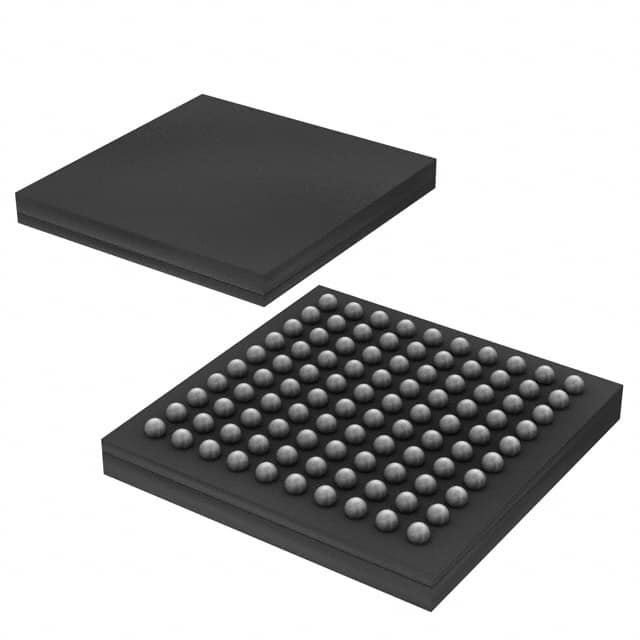
- Part No.:
- MAX32630IWG+
- Manufacturer:
- Analog Devices Inc./Maxim Integrated
- Category:
- Microcontrollers
- Package:
- 100-WFBGA, WLBGA
- Datasheet:
-
 MAX32630IWG+.pdf
- Description:
- IC MCU 32BIT 2MB FLASH 100WLP
- Quantity:
- Payment:

- Shipping:

Inventory:2,853
Please send an inquiry. Send us your inquiry, and we will respond immediately.
Product details
Overview
MAX32630IWG+ from Maxim Integrated is an ARM Cortex-M4F 32-bit microcontroller with floating-point unit, designed for ultra-low-power wearable medical and fitness applications. It delivers 96MHz peak performance, 2MB flash, 512KB SRAM, and integrated USB 2.0, AES-128/192/256, and a 10-bit delta-sigma ADC - enabling compact, battery-operated sensor hubs and medical patches.
For engineers reviewing the MAX32630IWG+ datasheet, MAX32630IWG+ pinout, MAX32630IWG+ application, or MAX32630IWG+ equivalent, this page provides verified technical context, power-mode trade-offs, GPIO mapping, peripheral timing constraints, and validated alternative MCUs for wearable system design.
Technical Context
The MAX32630IWG+ implements a dual-oscillator architecture: a factory-trimmed 96MHz internal oscillator (±0.24% over temperature) for high-performance operation and a 4MHz RC oscillator for always-on monitoring. Its Peripheral Management Unit (PMU) supports up to six autonomous power channels, enabling selective peripheral gating without CPU intervention.
Power management includes four distinct low-power modes: LP0 (600nA with RTC active), LP1 (3.5μW data retention with 5μs wake-up), LP2 (27μA/MHz dynamic current), and LP3 (106μA/MHz active current from cache). All modes retain full SRAM content except LP0, which preserves only RTC and critical registers.
Key Specifications
| Parameter | Value and Actual Design Meaning |
|---|---|
| Core | ARM Cortex-M4F with FPU, 96MHz max clock - enables real-time signal processing for biosensor algorithms. |
| Memory | 2MB flash / 512KB SRAM / 8KB instruction cache - supports complex firmware, OTA updates, and buffer-intensive sensor fusion. |
| ADC | 10-bit delta-sigma, 7.8ksps, 4-channel, 5V-tolerant AIN0–AIN1 - directly interfaces clinical-grade analog sensors without external level-shifting. |
| USB | Full-speed USB 2.0 with integrated transceiver and ±5% 3.3V supply tolerance - eliminates external PHY, reduces BOM count in diagnostic wearables. |
| Power Modes | LP0: 600nA (RTC on); LP1: 3.5μW (5μs wake-up); LP2: 27μA/MHz; LP3: 106μA/MHz - extends coin-cell life to >1 year in intermittent-monitoring patches. |
| I/O Voltage | VDDIO/VDDIOH: 1.8V–3.6V, independent from core (VDD12 = 1.2V) - simplifies mixed-voltage sensor interfacing and voltage-domain isolation. |
| Package | 100-ball WLP, 4.37mm × 4.37mm, 0.4mm pitch - meets footprint constraints of wrist-worn and epidermal medical devices. |
Pinout & Package
MAX32630IWG+ uses a 100-ball Wafer-Level Package (WLP) with 0.4mm ball pitch and 4.37mm × 4.37mm footprint. Ball layout follows JEDEC MO-220, land pattern referenced in Maxim Application Note 1891. Thermal resistance θJA = 38.9°C/W on four-layer board.
| Pin/Terminal | Circuit Role | Design Meaning |
|---|---|---|
| VDD12 | Core supply | 1.2V nominal input; must be decoupled with 1.0μF capacitor - powers ARM core, cache, and digital logic; defines active current efficiency (106μA/MHz). |
| VDD18 / VDDIO / VDDIOH | I/O domain supplies | Independent 1.8V–3.6V rails; VDDIOH ≥ VDDIO - enables mixed-voltage peripherals (e.g., 3.3V sensors + 1.8V display drivers) without level shifters. |
| DP / DM | USB differential pair | Integrated full-speed transceiver; internal weak pull-ups - eliminates external USB termination resistors and ESD protection diodes in cost-sensitive designs. |
| AIN0–AIN1 | Analog inputs | 5V-tolerant delta-sigma ADC inputs - accept direct connection to ECG/PPG front-ends without external attenuators or clamping diodes. |
| RSTN / SRSTN | Reset inputs | Hardware (active-low, VRTC-referenced) and software reset (VDDIO-referenced) - supports fail-safe recovery and debug-friendly soft resets without POR reinitialization. |
Key Features
| Feature | Design Value |
|---|---|
| SPIX Execute-in-Place engine | Enables direct code execution from external SPI flash, reducing SRAM pressure and supporting >2MB firmware without external memory controller. |
| Peripheral Management Unit (PMU) | 6-channel autonomous peripheral power control - cuts active current by disabling unused UART/I2C/SPI blocks without CPU polling or interrupt overhead. |
| Dual-clock system (96MHz + 4MHz) | Allows concurrent high-throughput data acquisition (96MHz) and sub-μA background monitoring (4MHz) - eliminates need for external RTC or wake-up timer ICs. |
| 16 PWM engines + 6×32-bit timers | Supports simultaneous LED dimming, motor control, and precise pulse-width modulation for optical biosensors (e.g., PPG LED drive). |
| AES-128/192/256 hardware accelerator | Offloads encryption from CPU, achieving <100μs AES-128 ECB encrypt/decrypt - secures BLE pairing keys and patient health data at rest/in transit. |
Applications
| Sports Watches | Fitness Monitors |
|---|---|
|
Use Scenario: GPS-enabled running watch with heart rate, accelerometer, and barometer sensing. IC Role / Device Role / Timing Role: Central MCU managing sensor fusion, display refresh, Bluetooth LE stack, and USB-C charging negotiation. Use Value: LP1 mode (3.5μW) maintains timekeeping and step counter during sleep; 96MHz burst mode processes raw IMU data in <2ms. |
Use Scenario: Arm-band fitness tracker with optical heart rate (PPG) and motion sensing. IC Role / Device Role / Timing Role: Signal processor for synchronous LED drive, ADC sampling, and real-time HRV analysis. Use Value: 10-bit delta-sigma ADC samples PPG at 7.8ksps with 58.5dB SNR; integrated AES encrypts biometric logs before BLE transmission. |
| Wearable Medical Patches | Portable Medical Devices |
|
Use Scenario: Single-use ECG patch transmitting 3-lead cardiac data via BLE to smartphone. IC Role / Device Role / Timing Role: Low-power data acquisition node with analog front-end control, flash logging, and secure wireless upload. Use Value: LP0 mode (600nA) sustains RTC and wake-up timer for 30-day shelf life; 5V-tolerant AIN0/AIN1 interface directly to instrumentation amplifier outputs. |
Use Scenario: Handheld spirometer with flow sensor, LCD, and USB diagnostics port. IC Role / Device Role / Timing Role: System controller handling analog pressure sensing, real-time volume calculation, and USB mass-storage emulation. Use Value: Integrated USB 2.0 transceiver enables plug-and-play PC diagnostics without external PHY; 2MB flash stores calibration tables and firmware updates. |
Equivalent & Alternatives
The following parts are listed as comparable options for similar microcontroller applications.
| Alternative Part | Technical Difference | Application Difference | Selection Advice |
|---|---|---|---|
| Nordic nRF52840-QIAA | No integrated ADC; BLE SoC with 1MB flash, no floating-point unit; USB requires external crystal; 64-pin QFN vs. 100-ball WLP. | Better RF integration for BLE-centric designs; lacks analog front-end for direct sensor interfacing. | Choose for pure wireless sensor nodes where RF performance outweighs analog capability and size constraints. |
| TI MSP432E401Y | Cortex-M4F at 120MHz; 1MB flash, 256KB SRAM; 12-bit SAR ADC (1MSPS); larger 128-pin LQFP package; higher active current (220μA/MHz). | Higher throughput for industrial data loggers; less suitable for sub-10mm wearable form factors. | Choose when higher ADC speed or larger memory is required and PCB area allows 12×12mm footprint. |
Compared with MAX32630IWG+, the nRF52840 offers superior wireless integration but requires external ADC and increases board area; the MSP432E401Y delivers higher compute bandwidth and ADC speed but consumes >2× more active current and occupies >2.5× more PCB area - making MAX32630IWG+ optimal for space- and battery-constrained medical wearables.
Availability
MAX32630IWG+ is available at Aetrix Electronics and suitable for sports watches, fitness monitors, and wearable medical patches requiring stable component supply across long-lifecycle healthcare programs.
Supply support for MAX32630IWG+ includes scheduled delivery planning, volume procurement assistance, BOM continuity management, traceable sourcing, and lifecycle availability coordination for OEM customers, industrial embedded developers, connected-device designers, and electronics production programs.
Manufacturer
Maxim Integrated (now part of Analog Devices) designs precision analog, mixed-signal, and high-reliability semiconductor solutions for industrial, medical, and communications markets.
The MAX32630IWG+ belongs to Maxim's ultra-low-power wearable microcontroller family, engineered specifically for battery-operated medical and fitness devices demanding sub-μA sleep currents, integrated security, and minimal footprint.
FAQ
What is the maximum operating frequency of the MAX32630IWG+?
The MAX32630IWG+ operates at up to 96MHz using its factory-trimmed internal oscillator, which maintains ±0.24% accuracy across -20°C to +85°C. This frequency is fully supported in all active power modes (LP2/LP3) and enables real-time execution of sensor fusion algorithms without external clock sources. The MAX32630IWG+ also supports a 4MHz RC oscillator for ultra-low-power background monitoring tasks.
Does the MAX32630IWG+ include hardware encryption acceleration?
Yes, the MAX32630IWG+ integrates a dedicated AES engine supporting AES-128, AES-192, and AES-256 in ECB and CBC modes. It performs encryption/decryption in hardware with latency under 100μs for 128-bit blocks, offloading the Cortex-M4F core and preserving deterministic timing for secure data logging and BLE pairing key management in medical applications.
What are the key differences between MAX32630IWG+ and MAX32631?
The MAX32630IWG+ is the base variant; the MAX32631 adds a Trust Protection Unit (TPU) with modular arithmetic accelerator (MAA), PRNG entropy source, and secure boot loader. The MAX32630IWG+ lacks MAA, secure key storage, and cryptographic key provisioning - making it suitable for non-regulated wearables, while MAX32631 targets HIPAA/FDA-compliant medical devices requiring certified secure boot and ECDSA signing.
How many general-purpose I/O pins does the MAX32630IWG+ support?
The MAX32630IWG+ provides up to 66 general-purpose I/O pins mapped across eight ports (P0–P8), with configurable drive strength, Schmitt-trigger inputs, and programmable pull-up/pull-down resistors (25kΩ typical, up to 1MΩ). These pins support multiple alternate functions including SPI, I2C, UART, PWM, and 1-Wire - enabling flexible peripheral expansion in space-constrained wearable designs.
What ADC specifications does the MAX32630IWG+ provide?
The MAX32630IWG+ features a 10-bit delta-sigma ADC with 4 input channels (AIN0–AIN3), 7.8ksps sample rate, 58.5dB SNR, and ±2 LSB INL. AIN0 and AIN1 are 5V-tolerant, allowing direct connection to clinical sensor front-ends. It supports internal bandgap or external reference (1.17–1.29V), and achieves 240µA active current with reference buffer enabled - optimized for precision, low-noise biosignal acquisition.
MAX32630IWG+ Specifications
- Product attributes
- Attribute value
- Manufacturer:
- Analog Devices Inc./Maxim Integrated
- Package/Case:
- 100-WFBGA, WLBGA
- Series:
- DARWIN
- Packaging:
- Strip
- Product Status:
- Active
- Programmable:
- Not Verified
- Core Processor:
- ARM® Cortex®-M4F
- Core Size:
- 32-Bit Single-Core
- Speed:
- 96MHz
- Connectivity:
- 1-Wire, I2C, SPI, UART/USART, USB
- Peripherals:
- Brown-out Detect/Reset, POR, PWM, WDT
- Number of I/O:
- 66
- Program Memory Size:
- 2MB (2M x 8)
- Program Memory Type:
- FLASH
- EEPROM Size:
- -
- RAM Size:
- 512K x 8
- Voltage - Supply (Vcc/Vdd):
- 1.14V ~ 3.6V
- Data Converters:
- A/D 4x10b
- Oscillator Type:
- Internal
- Operating Temperature:
- -20°C ~ 85°C (TA)
- Grade:
- -
- Qualification:
- -
- Mounting Type:
- Surface Mount
- Supplier Device Package:
MAX32630IWG+ FAQ
1.How can I place an order for MAX32630IWG+ through Aetrix?
Please submit a Request for Quotation (RFQ) for MAX32630IWG+ on Aetrix. Our sales agent will provide a competitive quotation and guide you through the order confirmation once you accept the terms.
2.Are the price and stock information for MAX32630IWG+ reliable?
The price and inventory of MAX32630IWG+ are updated periodically and may fluctuate due to market conditions. Stock and pricing data are typically refreshed every 24 hours. Quotation validity for MAX32630IWG+ is usually 5 days.
3.What payment methods are accepted for MAX32630IWG+?
We accept Wire Transfer, PayPal, Credit Card, Western Union, MoneyGram, and Escrow for MAX32630IWG+ transactions.
Note: Certain payment methods may incur a processing fee.
4.How is shipping managed for MAX32630IWG+?
MAX32630IWG+ orders can be shipped via leading logistics carriers, including DHL, UPS, FedEx, TNT, or Registered Mail.
Once your MAX32630IWG+ order is processed, you will receive an email with the shipment details and tracking number.
Note: Tracking information may take up to 24 hours to appear. Express delivery typically takes 3–5 business days.
5.How can I obtain technical support or documentation for MAX32630IWG+?
For technical support, including MAX32630IWG+ datasheets, pinout diagrams, or application guidance, please contact our engineering support team. They can provide detailed documentation and assistance for your MAX32630IWG+ requirements.
6.How does Aetrix verify that MAX32630IWG+ is sourced from the original manufacturer or authorized distributors?
All MAX32630IWG+ products on Aetrix are procured from qualified distributors and authorized channels. Our dedicated quality assurance team conducts strict verification, including traceability checks and, if necessary, third-party testing. This ensures that MAX32630IWG+ meets industry standards.
7.What is the process for return or replacement of MAX32630IWG+?
All MAX32630IWG+ units undergo pre-shipment inspection (PSI). If there is an issue with MAX32630IWG+, returns or replacements are accepted under the following conditions:
1.Quantity discrepancies, incorrect items, or visible external defects (such as breakage or corrosion), acknowledged by Aetrix.
2.The issue is reported within 90 days of delivery.
3.The MAX32630IWG+ part is unused and in its original packaging.
Return procedure for MAX32630IWG+:
1.Submit a request within 90 days.
2.Obtain a Return Material Authorization (RMA) from Aetrix.
MAX32630IWG+ Tags

-
ATTINY4-TSHR
Microchip Technology
-
ATTINY10-TSHR
Microchip Technology
-
ATTINY10-TS8R
Microchip Technology

-
ATTINY202-SSNR
Microchip Technology
-
ATTINY202-SSFR
Microchip Technology
-
ATTINY402-SSNR
Microchip Technology

-
PIC16F15213T-I/MF
Microchip Technology
-
PIC16F15213-E/MF
Microchip Technology

-
PIC10F200T-I/OT
Microchip Technology
-
ATTINY412-SSNR
Microchip Technology
-
PIC10F202T-I/OT
Microchip Technology

-
ATTINY404-SSNR
Microchip Technology
Tech Hub

A practical engineering guide to 3.3V and 5V logic compatibility, input thresholds, resistor dividers, translator ICs, MOSFET level shifting, I2C pull-ups, timing limits and power-sequencing risks.

The 74HC595 uses push-pull logic outputs, while the TPIC6B595 uses 50 V open-drain DMOS sinks for higher-power loads. This guide compares timing, current limits, 3.3 V interfacing, load wiring, thermal…

The 74HC595 converts serial data into eight stable parallel outputs. This guide covers pin functions, shift and storage timing, OE and MR behavior, drive-current limits, cascading, voltage compatibilit…

A technical comparison of level-sensitive latches and edge-triggered flip-flops, covering timing windows, setup and hold limits, master–slave operation, time borrowing, race-through, HDL inference and…

A D latch stores one bit while Enable controls when data can pass. This reference covers gate-level operation, truth tables, transparency, setup and hold timing, LE versus OE, common ICs and practical …

An SR latch stores one bit through cross-coupled feedback. This engineering reference covers NOR and NAND implementations, truth tables, forbidden-state recovery, gated operation, switch debouncing, fa…

Latch circuits retain one bit through feedback. This technical reference covers SR and D latches, truth tables, transparency, timing limits, latch-versus-flip-flop behavior, applications and common log…

An engineering guide to LED driver operation, constant-current and constant-voltage outputs, linear and switching topologies, dimming, IC selection, calculations, replacement compatibility, and fault c…

Operational amplifier guide covering op amp basics, feedback, ideal vs real op amps, common configurations, buffer circuits, offset, bias current, gain-bandwidth, slew rate, rail-to-rail limits and sel…

Jumper cables guide covering safe connection order, red and black clamp placement, final ground connection, cable gauge, length, clamp quality, copper vs CCA cables, jump starter comparison and battery…


