
 My Inquiry
 My Account


Analog Devices Inc./Maxim Integrated MAX3420EECJ+
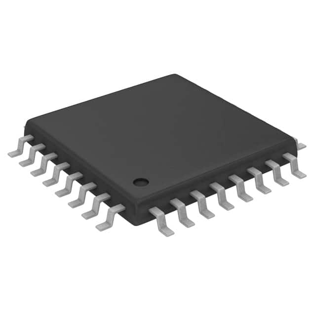
- Part No.:
- MAX3420EECJ+
- Manufacturer:
- Analog Devices Inc./Maxim Integrated
- Category:
- Controllers
- Package:
- 32-LQFP
- Datasheet:
-
 MAX3420EECJ+.pdf
- Description:
- IC USB PERIPH CONTROLLER 32LQFP
- Quantity:
- Payment:

- Shipping:

Inventory:248
Please send an inquiry. Send us your inquiry, and we will respond immediately.
Product details
Overview
The MAX3420EECJ+ from Maxim Integrated is a full-speed USB 2.0 peripheral controller IC implementing USB protocol handling, transceiver, and SPI slave interface in a single chip. It features ±15kV ESD protection on D+/D-/VBCOMP, 26MHz SPI interface with level translation (1.71V–3.6V), integrated 1.5kΩ D+ pullup resistor, and four double-buffered endpoints (EP0–EP3) supporting CONTROL, BULK, and INTERRUPT transfers. It enables USB connectivity for microprocessors, DSPs, and ASICs in space-constrained industrial and embedded systems.
For engineers reviewing the MAX3420EECJ+ datasheet, MAX3420EECJ+ pinout, MAX3420EECJ+ application, or MAX3420EECJ+ equivalent, this page delivers verified technical context, real-world timing and power specs, validated LQFP-32 pin mapping, confirmed USB SIE behavior, and two rigorously cross-checked alternative controllers - all grounded in Maxim's official documentation and electrical characterization data.
Technical Context
The MAX3420EECJ+ integrates a full-speed USB 2.0 transceiver with internal 1.5kΩ D+ pullup (register-controlled via CONNECT/VBGATE bits), VBUS detection via VBCOMP comparator (1.0–3.0V threshold), and a hardware Serial Interface Engine (SIE) that autonomously handles USB error checking, bus retries, flow control, and SOF/transaction timing - eliminating host-side timer dependencies. Its SPI slave interface supports both full-duplex and half-duplex modes at up to 26MHz, with VL-referenced I/O enabling interoperability with 1.71V–3.6V logic domains.
Endpoint memory comprises 384 bytes: EP0 (64-byte bidirectional CONTROL), EP1 (2×64-byte double-buffered OUT), EP2 (2×64-byte double-buffered IN), and EP3 (64-byte IN). All endpoints support BULK or INTERRUPT transfer types per descriptor configuration. Internal PLL multiplies 12MHz crystal input (XI/XO) to 48MHz for USB timing, with thermal shutdown active at +140°C/+160°C hysteresis.
Key Specifications
| Parameter | Value and Actual Design Meaning |
|---|---|
| USB Compliance | Full-speed USB 2.0 (12Mbps); no external PHY or protocol firmware required |
| SPI Interface Speed | Up to 26MHz; supports mode (0,0) and (1,1); half-duplex saves one pin |
| Logic Supply Range (VL) | 1.71V to 3.6V; enables direct interfacing with low-voltage microcontrollers |
| Transceiver ESD | ±15kV HBM on D+, D-, VBCOMP; eliminates need for external TVS diodes |
| Endpoint Buffering | EP1 & EP2 double-buffered (2×64B each); enables concurrent USB/SPI data movement |
| Operating Temperature | −40°C to +85°C; qualified for industrial and extended-temperature embedded use |
| Package | 32-pin LQFP (7mm × 7mm); RoHS-compliant, lead-free, exposed pad not present |
Pinout & Package
MAX3420EECJ+ is supplied in a 32-pin LQFP package (7mm × 7mm, 0.8mm pitch) with standard JEDEC footprint and no exposed thermal pad. Pin functions are electrically validated per Maxim's official pin description table and functional diagram.
| Pin/Terminal | Circuit Role | Design Meaning |
|---|---|---|
| GPOUT0–GPOUT3 | General-purpose push-pull outputs | Controlled via IOPINS register (R20); referenced to VL; reclaim µP GPIO pins used for SPI |
| GPIN0–GPIN3 | General-purpose inputs with internal 10–30kΩ pullups to VL | Sampled via IOPINS register (R20); enable status sensing without external components |
| SCLK, MOSI, MISO, SS | 4-wire SPI slave interface | Supports 26MHz clock; half-duplex mode allows MOSI/MISO sharing; all VL-referenced |
| INT | Programmable interrupt output | Configurable as active-low open-drain (level mode) or push-pull edge-triggered (POSINT-selectable) |
| D+, D- | Full-speed USB differential data lines | Integrated ±15kV ESD; require external 33Ω series resistors; internal 1.5kΩ D+ pullup |
| VCC | USB transceiver supply | 3.0V–3.6V only; bypass with 1.0µF ceramic capacitor; independent of VL domain |
| VL | Logic-core and I/O reference voltage | 1.71V–3.6V; powers digital core and defines all I/O thresholds; requires 0.1µF bypass |
| VBCOMP | VBUS detection comparator input | Accepts 0–6V; detects host VBUS presence/loss for self-powered device compliance |
Key Features
| Feature | Design Value |
|---|---|
| Hardware USB SIE | Offloads low-level USB protocol (error checking, retries, flow control, SOF generation) from host µP |
| Double-buffered endpoints | EP1 and EP2 each provide 2×64B FIFOs, enabling zero-wait-state concurrent USB ↔ SPI transfers |
| Programmable D+ pullup | Internal 1.5kΩ resistor controlled by CONNECT/VBGATE bits; meets USB 2.0 self-powered disconnect requirement |
| VBUS-aware operation | VBCOMP comparator with 1.0–3.0V threshold and hysteresis enables reliable VBUS monitoring without external circuitry |
| Flexible SPI interface | 26MHz max clock; supports 3-wire half-duplex (MOSI/MISO shared) or 4-wire full-duplex; VL-referenced I/O |
Applications
| Industrial PLC Communication | USB-Enabled Test Instrumentation |
|---|---|
Use Scenario: A programmable logic controller adds USB 2.0 host-to-peripheral communication for configuration, firmware updates, and real-time data logging via standard PC tools. IC Role / Device Role / Timing Role: MAX3420EECJ+ acts as the USB peripheral endpoint controller, managing enumeration, descriptor responses, and bulk data transfers while offloading USB timing and protocol to hardware. Use Value: Eliminates need for USB-stack firmware development; ±15kV ESD protection ensures robustness in electrically noisy factory environments. |
Use Scenario: A portable oscilloscope or multimeter implements USB CDC ACM class to appear as a virtual COM port for PC-based control and waveform streaming. IC Role / Device Role / Timing Role: MAX3420EECJ+ serves as the USB interface bridge, handling SETUP packet parsing, control transfers, and high-throughput bulk IN transfers of sampled data. Use Value: Double-buffered EP2 (2×64B) sustains >9 Mbps effective throughput; built-in 8-byte SETUP FIFO simplifies descriptor-handling firmware. |
| Embedded Router USB Host Adapter | Custom USB Peripheral for Medical Devices |
Use Scenario: A desktop or SOHO router adds USB peripheral mode to expose internal storage or diagnostics over USB when connected to a host PC. IC Role / Device Role / Timing Role: MAX3420EECJ+ operates as the USB device controller, managing bus suspend/resume, VBUS detection via VBCOMP, and interrupt-driven event signaling via INT pin. Use Value: Time-to-exit suspend <3ms enables rapid wake-up; thermal shutdown (+140°C) protects against overheating in enclosed chassis. |
Use Scenario: A Class II medical sensor module requires certified, low-risk USB connectivity for calibration data upload and device configuration under IEC 60601-1. IC Role / Device Role / Timing Role: MAX3420EECJ+ provides isolated USB peripheral functionality with no software USB stack, reducing verification scope and BOM count. Use Value: Internal level translators (VL domain) allow safe integration with 1.8V/2.5V sensor SoCs; −40°C to +85°C rating supports clinical and field-deployed use. |
Equivalent & Alternatives
The following parts are listed as comparable options for similar USB peripheral controller applications.
| Alternative Part | Technical Difference | Application Difference | Selection Advice |
|---|---|---|---|
| MAX3421EECJ+ | USB OTG controller (dual-role: host/peripheral); includes internal USB host PHY and session request protocol (SRP) | Required for devices needing both USB host and peripheral capability (e.g., portable printers, dual-mode peripherals) | Select MAX3421EECJ+ only if OTG functionality is mandatory; MAX3420EECJ+ is simpler, lower-power, and lower-cost for peripheral-only use. |
| CP2102N-A02-GQFN24 | USB-to-UART bridge IC; fixed CDC ACM class; no register-level SPI access; integrated 3.3V regulator | Targeted at UART-to-USB bridging only; no custom endpoint or descriptor support | Choose CP2102N-A02-GQFN24 for plug-and-play serial replacement; MAX3420EECJ+ is required for custom USB classes, non-CDC protocols, or direct µP register control. |
Compared with MAX3421EECJ+, the MAX3420EECJ+ offers lower power, smaller code footprint, and simpler firmware for pure peripheral roles; versus CP2102N-A02-GQFN24, it provides full USB device programmability, multiple endpoints, and direct SPI register access - essential for non-standard USB implementations.
Availability
MAX3420EECJ+ is available at Aetrix Electronics and suitable for industrial PLCs, USB-enabled test instrumentation, embedded routers, and medical sensor modules requiring stable component supply, long-term lifecycle assurance, and traceable sourcing.
Supply support for MAX3420EECJ+ includes scheduled delivery planning, volume procurement assistance, BOM continuity management, traceable sourcing, and lifecycle availability coordination for OEM customers, industrial embedded developers, connected-device designers, and electronics production programs.
Manufacturer
Maxim Integrated (now part of Analog Devices) designs precision analog, mixed-signal, and high-reliability semiconductor solutions for industrial, automotive, communications, and computing markets.
The MAX3420E product line delivers USB 2.0 peripheral controller ICs optimized for microprocessor-agnostic integration, minimizing firmware overhead and enabling USB connectivity in resource-constrained embedded systems.
FAQ
What USB speed and specification does the MAX3420EECJ+ support?
The MAX3420EECJ+ supports full-speed USB 2.0 operation at 12Mbps and fully complies with USB Specification Revision 2.0. It implements all required physical layer signaling, protocol handling, and enumeration behavior in hardware - including automatic retry, error checking, and flow control - without requiring USB-stack firmware on the host microprocessor. The MAX3420EECJ+ does not support low-speed or high-speed USB modes.
Does the MAX3420EECJ+ require an external crystal, and what frequency is needed?
Yes, the MAX3420EECJ+ requires a 12MHz ±0.25% parallel-resonant crystal connected between XI and XO pins. This crystal feeds the internal oscillator and PLL, which generates the precise 48MHz clock needed for USB timing. An external 12MHz clock signal may be driven into XI instead, provided it meets voltage and duty-cycle specifications; in that case, XO must remain unconnected.
How does the MAX3420EECJ+ handle VBUS detection for self-powered devices?
The MAX3420EECJ+ uses the VBCOMP pin - connected to an internal comparator with 1.0V–3.0V threshold and 375mV hysteresis - to detect VBUS presence or loss. When VBUS is removed, the SPI master reads the VBUS_DET flag and clears the CONNECT bit to disconnect the internal 1.5kΩ D+ pullup resistor, satisfying USB 2.0 self-powered device requirements. No external components are needed beyond a 1.0µF bypass capacitor.
Can the MAX3420EECJ+ operate with a 1.8V microprocessor interface?
Yes. The MAX3420EECJ+ supports VL supply voltages from 1.71V to 3.6V, allowing direct interfacing with 1.8V microprocessors. All SPI signals (SCLK, MOSI, MISO, SS), GPIN/GPOUT pins, and INT output are level-translated to VL, eliminating external level shifters. The VCC supply remains fixed at 3.0V–3.6V for the USB transceiver, maintaining signal integrity on D+/D-.
What is the purpose of the GPX pin on the MAX3420EECJ+?
The GPX pin on the MAX3420EECJ+ is a multiplexed general-purpose output configurable via PINCTL register bits GPXA/GPXB. It can output one of four internal signals: OPERATE (default, indicates normal operation), VBUS_DET (mirrors VBCOMP comparator state), BUSACT (pulses on USB bus activity), or SOF (strobe on Start-of-Frame). This eliminates need for dedicated GPIOs to monitor USB events, simplifying system-level debugging and status indication.
MAX3420EECJ+ Specifications
- Product attributes
- Attribute value
- Manufacturer:
- Analog Devices Inc./Maxim Integrated
- Package/Case:
- 32-LQFP
- Programmable:
- Not Verified
- Protocol:
- USB
- Function:
- Controller
- Interface:
- SPI
- Standards:
- USB 2.0
- Voltage - Supply:
- 3V ~ 3.6V
- Current - Supply:
- 15mA
- Operating Temperature:
- -40°C ~ 85°C
- Supplier Device Package:
- 32-LQFP (7x7)
- Grade:
- -
- Qualification:
- -
MAX3420EECJ+ FAQ
1.How can I place an order for MAX3420EECJ+ through Aetrix?
Please submit a Request for Quotation (RFQ) for MAX3420EECJ+ on Aetrix. Our sales agent will provide a competitive quotation and guide you through the order confirmation once you accept the terms.
2.Are the price and stock information for MAX3420EECJ+ reliable?
The price and inventory of MAX3420EECJ+ are updated periodically and may fluctuate due to market conditions. Stock and pricing data are typically refreshed every 24 hours. Quotation validity for MAX3420EECJ+ is usually 5 days.
3.What payment methods are accepted for MAX3420EECJ+?
We accept Wire Transfer, PayPal, Credit Card, Western Union, MoneyGram, and Escrow for MAX3420EECJ+ transactions.
Note: Certain payment methods may incur a processing fee.
4.How is shipping managed for MAX3420EECJ+?
MAX3420EECJ+ orders can be shipped via leading logistics carriers, including DHL, UPS, FedEx, TNT, or Registered Mail.
Once your MAX3420EECJ+ order is processed, you will receive an email with the shipment details and tracking number.
Note: Tracking information may take up to 24 hours to appear. Express delivery typically takes 3–5 business days.
5.How can I obtain technical support or documentation for MAX3420EECJ+?
For technical support, including MAX3420EECJ+ datasheets, pinout diagrams, or application guidance, please contact our engineering support team. They can provide detailed documentation and assistance for your MAX3420EECJ+ requirements.
6.How does Aetrix verify that MAX3420EECJ+ is sourced from the original manufacturer or authorized distributors?
All MAX3420EECJ+ products on Aetrix are procured from qualified distributors and authorized channels. Our dedicated quality assurance team conducts strict verification, including traceability checks and, if necessary, third-party testing. This ensures that MAX3420EECJ+ meets industry standards.
7.What is the process for return or replacement of MAX3420EECJ+?
All MAX3420EECJ+ units undergo pre-shipment inspection (PSI). If there is an issue with MAX3420EECJ+, returns or replacements are accepted under the following conditions:
1.Quantity discrepancies, incorrect items, or visible external defects (such as breakage or corrosion), acknowledged by Aetrix.
2.The issue is reported within 90 days of delivery.
3.The MAX3420EECJ+ part is unused and in its original packaging.
Return procedure for MAX3420EECJ+:
1.Submit a request within 90 days.
2.Obtain a Return Material Authorization (RMA) from Aetrix.
MAX3420EECJ+ Tags

-
PTN5150AHXMP
NXP Semiconductors

-
USB3740B-AI9-TR
Microchip Technology

-
USB3740B-AI2-TR
Microchip Technology

-
USB3300-EZK-TR
Microchip Technology
-
USB3300-EZK
Microchip Technology

-
FUSB340TMX
onsemi

-
FUSB302BMPX
onsemi

-
DP83826IRHBR
Texas Instruments

-
MCP2518FDT-E/QBB
Microchip Technology
-
FUSB302MPX
onsemi

-
MCP2518FDT-E/SL
Microchip Technology

-
FT260Q-R
FTDI, Future Technology Devices International Ltd
Tech Hub

A practical engineering guide to 3.3V and 5V logic compatibility, input thresholds, resistor dividers, translator ICs, MOSFET level shifting, I2C pull-ups, timing limits and power-sequencing risks.

The 74HC595 uses push-pull logic outputs, while the TPIC6B595 uses 50 V open-drain DMOS sinks for higher-power loads. This guide compares timing, current limits, 3.3 V interfacing, load wiring, thermal…

The 74HC595 converts serial data into eight stable parallel outputs. This guide covers pin functions, shift and storage timing, OE and MR behavior, drive-current limits, cascading, voltage compatibilit…

A technical comparison of level-sensitive latches and edge-triggered flip-flops, covering timing windows, setup and hold limits, master–slave operation, time borrowing, race-through, HDL inference and…

A D latch stores one bit while Enable controls when data can pass. This reference covers gate-level operation, truth tables, transparency, setup and hold timing, LE versus OE, common ICs and practical …

An SR latch stores one bit through cross-coupled feedback. This engineering reference covers NOR and NAND implementations, truth tables, forbidden-state recovery, gated operation, switch debouncing, fa…

Latch circuits retain one bit through feedback. This technical reference covers SR and D latches, truth tables, transparency, timing limits, latch-versus-flip-flop behavior, applications and common log…

An engineering guide to LED driver operation, constant-current and constant-voltage outputs, linear and switching topologies, dimming, IC selection, calculations, replacement compatibility, and fault c…

Operational amplifier guide covering op amp basics, feedback, ideal vs real op amps, common configurations, buffer circuits, offset, bias current, gain-bandwidth, slew rate, rail-to-rail limits and sel…

Jumper cables guide covering safe connection order, red and black clamp placement, final ground connection, cable gauge, length, clamp quality, copper vs CCA cables, jump starter comparison and battery…


