
 My Inquiry
 My Account


Analog Devices Inc./Maxim Integrated MAX366CSA+T
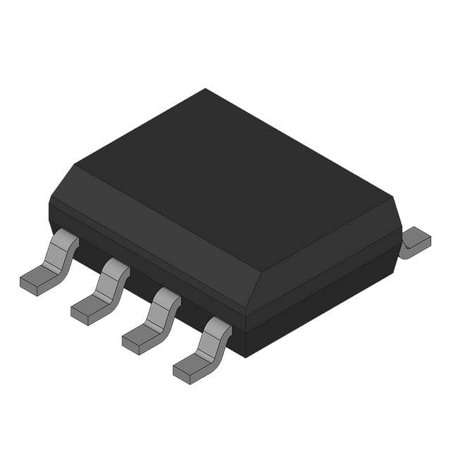
- Part No.:
- MAX366CSA+T
- Manufacturer:
- Analog Devices Inc./Maxim Integrated
- Category:
- Mixed Technology
- Package:
- 8-SOIC (0.154", 3.90mm Width)
- Datasheet:
-
 MAX366CSA+T.pdf
- Description:
- TVS DEVICE MIXED 40V 8SOIC
- Quantity:
- Payment:

- Shipping:

Inventory:2,898
Please send an inquiry. Send us your inquiry, and we will respond immediately.
Product details
Overview
MAX366CSA+T from Maxim Integrated is a triple two-terminal analog signal-line protector IC designed for series insertion in sensitive analog signal paths. It provides ±40V overvoltage protection, 100Ω max on-resistance with power applied, and <1nA leakage at +25°C, enabling robust fault containment in data-acquisition front-ends and hot-insertion sensor interfaces.
For engineers reviewing the MAX366CSA+T datasheet, MAX366CSA+T pinout, MAX366CSA+T application, or MAX366CSA+T equivalent, this device serves as a voltage-sensitive MOSFET array that automatically clamps fault currents without control logic-critical for protecting op-amp inputs, ADC drivers, and precision references during power sequencing, brownouts, or external fault transients.
Technical Context
The MAX366CSA+T implements three independent symmetrical two-terminal protectors using enhancement-mode N- and P-channel FETs. Each protector operates without directionality: IN/OUT pins are electrically identical and interchangeable. During normal operation (signal within ~1.5V of supply rails), it presents a low-impedance path (<100Ω); when signal exceeds rail limits, internal FET gate thresholds trigger high-impedance limiting behavior.
It requires bipolar (±2.25V to ±18V) or unipolar (4.5V to 36V) supplies and draws <1µA quiescent current. Fault response is supply-driven-not externally controlled-and isolates up to ±40V with zero bias (V+ = V− = 0V), while maintaining polarity integrity and eliminating glitches or reversals during fault entry/exit.
Key Specifications
| Parameter | Value and Actual Design Meaning |
|---|---|
| Protector Count | Three independent, symmetrical two-terminal protectors per package |
| Overvoltage Protection | ±40V maximum fault voltage tolerance-protects against transients beyond supply rails, including during power-off |
| On-Resistance (RIN-OUT) | ≤100Ω at ±10V supplies-minimizes signal attenuation in high-impedance analog paths |
| Signal-Path Leakage | <1nA at +25°C under normal conditions-preserves accuracy in µV-level instrumentation circuits |
| Fault Knee Voltage | ~1.3V below V+, ~2.0V above V−-defines clamping threshold and ensures safe output voltage during faults |
| Supply Range | Unipolar: 4.5V to 36V; Bipolar: ±2.25V to ±18V-supports industrial, process control, and ATE power architectures |
| Power-Off Isolation | Open-circuit path with >1000MΩ resistance-prevents cross-talk and backfeeding between powered/unpowered subsystems |
Pinout & Package
MAX366CSA+T is housed in an 8-pin SO (Small Outline) package with 150-mil body width, RoHS-compliant lead finish, and standard JEDEC MS-012AC footprint. Pin 1 is marked by a beveled corner or dot; leads are gull-wing shaped with 1.27mm pitch.
| Pin | Circuit Role | Design Meaning |
|---|---|---|
| 1, 2, 3 | Signal Terminal (IN/OUT) | Interchangeable input/output for Protector 1, 2, 3-no directionality; each pair forms a bidirectional protected path |
| 4 | Positive Supply (V+) | Connects to most positive rail; biases N-channel FET gates and defines upper fault knee |
| 5, 6, 7 | Signal Terminal (OUT/IN) | Interchangeable output/input for Protector 1, 2, 3-electrically identical to Pins 1–3; full symmetry enables flexible layout |
| 8 | Negative Supply (V−) | Connects to most negative rail (or ground in single-supply); biases P-channel FET gate and defines lower fault knee |
Key Features
| Feature | Design Value |
|---|---|
| Automatic fault response | No control lines, programming, or external circuitry required-protection activates inherently based on supply and signal voltage relationship |
| Symmetrical terminal architecture | Pins 1–3 and 5–7 are functionally identical and swappable-eliminates routing constraints and simplifies PCB layout |
| Power-off open-circuit behavior | Zero bias yields virtual open circuit-enables safe hot-swap and modular system isolation without added switches or relays |
| Low-leakage fault containment | <1nA leakage during normal operation and <1000nA during fault-preserves integrity of high-Z sensor outputs and reference nodes |
| Bipolar/single-supply flexibility | Operates from ±2.25V to ±18V or 4.5V to 36V-supports legacy ±15V instrumentation and modern 5V/12V industrial systems |
Applications
| Process Control Signal Conditioning | Hot-Insertion Sensor Interface |
|---|---|
Use Scenario: Analog signals from remote temperature, pressure, or flow sensors traverse long cables into PLC I/O modules where ESD, load dump, or miswiring may inject ±30V transients. IC Role / Device Role / Timing Role: Series-connected protector placed between cable connector and precision amplifier input-acts as self-regulating voltage clamp during fault events. Use Value: Prevents latch-up or permanent damage to downstream op-amps and ADCs while maintaining ≤100Ω signal path impedance during normal operation. |
Use Scenario: Field-replaceable sensor cards are inserted into live backplanes carrying ±12V and 5V rails, risking supply-rail overshoot and cross-coupling during mating. IC Role / Device Role / Timing Role: Three independent protectors guard differential analog inputs on each card-activated only when local V+/V− are present, ensuring isolation before power stabilization. Use Value: Enables true hot-swap capability without sequenced power enable circuitry; eliminates need for mechanical interlocks or manual power cycling. |
| Data-Acquisition Front-End Protection | Redundant System Cross-Connection |
Use Scenario: High-resolution 24-bit delta-sigma ADCs receive low-level mV-range signals from strain gauges or thermocouples in test equipment subject to accidental probe contact with chassis ground. IC Role / Device Role / Timing Role: Placed directly at ADC input pins to limit fault current and clamp output voltage to safe levels-operates transparently during acquisition windows. Use Value: Maintains sub-µV offset stability and THD performance while guaranteeing survival against ±35V faults-no calibration drift or post-fault recalibration needed. |
Use Scenario: Dual-redundant controllers share analog status signals via backplane; one channel must remain functional even if the other experiences short-to-rail failure. IC Role / Device Role / Timing Role: MAX366CSA+T isolates each controller's analog monitoring line-blocks fault propagation while allowing normal signal pass-through under healthy conditions. Use Value: Achieves fail-safe signal coupling without optocouplers or discrete FETs-reduces BOM count, board area, and timing skew between redundant paths. |
Equivalent & Alternatives
The following parts are listed as comparable options for similar analog signal-line protection applications.
| Alternative Part | Technical Difference | Application Difference | Selection Advice |
|---|---|---|---|
| MAX366CPA+ | 8-pin plastic DIP package; same electrical specs but higher thermal resistance (727mW vs. 471mW SO rating) and wider operating temp range (0°C to +70°C only) | Preferred for through-hole prototyping or legacy DIP-based systems; less suitable for high-density SMT production | Select MAX366CPA+ only when DIP footprint is mandated; MAX366CSA+T offers superior thermal performance and smaller PCB footprint |
| MAX367CSA+ | Eight-protector version in same 8-SO package; shares identical per-protector specs but doubles channel count per unit area | Used where higher channel density is required-e.g., multi-channel DAQ modules or dense sensor arrays-without increasing board space | Choose MAX366CSA+T when exactly three protected paths are needed; MAX367CSA+ adds cost and complexity if unused channels remain idle |
Compared with MAX366CPA+, the MAX366CSA+T delivers better thermal management and surface-mount compatibility; compared with MAX367CSA+, it avoids over-provisioning and reduces parasitic capacitance per channel in low-noise analog designs.
Availability
MAX366CSA+T is available at Aetrix Electronics and suitable for process control systems, hot-insertion sensor interfaces, and data-acquisition front-ends requiring stable component supply across extended product lifecycles.
Supply support for MAX366CSA+T includes scheduled delivery planning, volume procurement assistance, BOM continuity management, traceable sourcing, and lifecycle availability coordination for OEM customers, industrial embedded developers, connected-device designers, and electronics production programs.
Manufacturer
Maxim Integrated (now part of Analog Devices) is a fabless semiconductor company specializing in high-performance analog, mixed-signal, and power-management ICs for industrial, communications, and computing markets.
The MAX366CSA+T belongs to Maxim's signal-line protection product line, engineered specifically to safeguard precision analog interfaces against real-world overvoltage threats-including power sequencing errors, ESD, and cable-induced transients-without degrading signal fidelity.
FAQ
What is the maximum continuous fault voltage the MAX366CSA+T can withstand?
The MAX366CSA+T supports up to ±40V fault voltage relative to its supply rails-even with zero bias (V+ = V− = 0V). This rating is validated per Absolute Maximum Ratings and confirmed in Typical Operating Characteristics curves showing path resistance rise above ±35V under off-state conditions. The device achieves this via intrinsic FET gate-threshold behavior, not external clamping diodes.
Can the MAX366CSA+T be used with single-supply systems?
Yes, the MAX366CSA+T operates with unipolar supplies from 4.5V to 36V. In single-supply mode, V− is tied to ground, and the lower fault knee occurs ~2V above ground. Signals below ~2V enter fault condition, so design must ensure valid analog range stays above this threshold-e.g., using biased AC-coupled inputs or rail-to-rail op-amps.
Does the MAX366CSA+T require external components to function?
No, the MAX366CSA+T requires only V+ and V− connections and series placement in the signal path-no resistors, capacitors, or control logic. Its protection behavior is fully autonomous, governed by internal FET thresholds and supply voltages. External components are optional only for specialized cases like high-Z load stabilization or surge suppression staging.
How does the MAX366CSA+T behave during power-up and power-down transitions?
During power ramp-up, the MAX366CSA+T remains in high-impedance fault state until V+ and V− exceed the signal voltage by ~1.5V; output follows input only after exit from fault. During ramp-down, it re-enters fault state smoothly-no glitches or polarity reversal occur. This behavior is inherent to its FET-based architecture and documented in Low-Voltage Operation and Power Off sections.
Is the MAX366CSA+T pin-compatible with other members of the MAX366/MAX367 family?
Yes, all MAX366 variants-including MAX366CSA+T, MAX366CPA+, and MAX366C/D-share identical 8-pin SO, DIP, and die pinouts. Pin functions (IN1/OUT1 through IN3/OUT3, V+, V−) are fixed across packages. However, MAX367 variants use 18-pin packages and are not pin-compatible; they offer eight protectors instead of three.
MAX366CSA+T Specifications
- Product attributes
- Attribute value
- Manufacturer:
- Analog Devices Inc./Maxim Integrated
- Package/Case:
- 8-SOIC (0.154", 3.90mm Width)
- Series:
- -
- Packaging:
- Tape & Reel (TR)
- Product Status:
- Active
- Voltage - Clamping:
- ±40V
- Technology:
- Mixed Technology
- Number of Circuits:
- 3
- Applications:
- General Purpose
- Grade:
- -
- Qualification:
- -
- Mounting Type:
- Surface Mount
- Supplier Device Package:
- 8-SOIC
MAX366CSA+T FAQ
1.How can I place an order for MAX366CSA+T through Aetrix?
Please submit a Request for Quotation (RFQ) for MAX366CSA+T on Aetrix. Our sales agent will provide a competitive quotation and guide you through the order confirmation once you accept the terms.
2.Are the price and stock information for MAX366CSA+T reliable?
The price and inventory of MAX366CSA+T are updated periodically and may fluctuate due to market conditions. Stock and pricing data are typically refreshed every 24 hours. Quotation validity for MAX366CSA+T is usually 5 days.
3.What payment methods are accepted for MAX366CSA+T?
We accept Wire Transfer, PayPal, Credit Card, Western Union, MoneyGram, and Escrow for MAX366CSA+T transactions.
Note: Certain payment methods may incur a processing fee.
4.How is shipping managed for MAX366CSA+T?
MAX366CSA+T orders can be shipped via leading logistics carriers, including DHL, UPS, FedEx, TNT, or Registered Mail.
Once your MAX366CSA+T order is processed, you will receive an email with the shipment details and tracking number.
Note: Tracking information may take up to 24 hours to appear. Express delivery typically takes 3–5 business days.
5.How can I obtain technical support or documentation for MAX366CSA+T?
For technical support, including MAX366CSA+T datasheets, pinout diagrams, or application guidance, please contact our engineering support team. They can provide detailed documentation and assistance for your MAX366CSA+T requirements.
6.How does Aetrix verify that MAX366CSA+T is sourced from the original manufacturer or authorized distributors?
All MAX366CSA+T products on Aetrix are procured from qualified distributors and authorized channels. Our dedicated quality assurance team conducts strict verification, including traceability checks and, if necessary, third-party testing. This ensures that MAX366CSA+T meets industry standards.
7.What is the process for return or replacement of MAX366CSA+T?
All MAX366CSA+T units undergo pre-shipment inspection (PSI). If there is an issue with MAX366CSA+T, returns or replacements are accepted under the following conditions:
1.Quantity discrepancies, incorrect items, or visible external defects (such as breakage or corrosion), acknowledged by Aetrix.
2.The issue is reported within 90 days of delivery.
3.The MAX366CSA+T part is unused and in its original packaging.
Return procedure for MAX366CSA+T:
1.Submit a request within 90 days.
2.Obtain a Return Material Authorization (RMA) from Aetrix.
MAX366CSA+T Tags
-
ESD03A5V5R17V
Stackpole Electronics Inc
-
ESDU02A5V5R17V
Stackpole Electronics Inc
-
0603ESDA-MLP7
Eaton - Electronics Division
.jpg)
-
0603ESDA2-TR2
Eaton - Electronics Division
-
PS04LTVA1
Eaton - Electronics Division
.jpg)
-
0402ESDA-MLP1
Eaton - Electronics Division
.jpg)
-
0402ESDA-MLP7
Eaton - Electronics Division
-
TPD2S017DBVR
Texas Instruments
.jpg)
-
V2F105A150Y2EDP
KYOCERA AVX
-
82307050029
Würth Elektronik
-
NCP360SNT1G
onsemi
-
V2F118A400Y2EDP
KYOCERA AVX
Tech Hub

A practical engineering guide to 3.3V and 5V logic compatibility, input thresholds, resistor dividers, translator ICs, MOSFET level shifting, I2C pull-ups, timing limits and power-sequencing risks.

The 74HC595 uses push-pull logic outputs, while the TPIC6B595 uses 50 V open-drain DMOS sinks for higher-power loads. This guide compares timing, current limits, 3.3 V interfacing, load wiring, thermal…

The 74HC595 converts serial data into eight stable parallel outputs. This guide covers pin functions, shift and storage timing, OE and MR behavior, drive-current limits, cascading, voltage compatibilit…

A technical comparison of level-sensitive latches and edge-triggered flip-flops, covering timing windows, setup and hold limits, master–slave operation, time borrowing, race-through, HDL inference and…

A D latch stores one bit while Enable controls when data can pass. This reference covers gate-level operation, truth tables, transparency, setup and hold timing, LE versus OE, common ICs and practical …

An SR latch stores one bit through cross-coupled feedback. This engineering reference covers NOR and NAND implementations, truth tables, forbidden-state recovery, gated operation, switch debouncing, fa…

Latch circuits retain one bit through feedback. This technical reference covers SR and D latches, truth tables, transparency, timing limits, latch-versus-flip-flop behavior, applications and common log…

An engineering guide to LED driver operation, constant-current and constant-voltage outputs, linear and switching topologies, dimming, IC selection, calculations, replacement compatibility, and fault c…

Operational amplifier guide covering op amp basics, feedback, ideal vs real op amps, common configurations, buffer circuits, offset, bias current, gain-bandwidth, slew rate, rail-to-rail limits and sel…

Jumper cables guide covering safe connection order, red and black clamp placement, final ground connection, cable gauge, length, clamp quality, copper vs CCA cables, jump starter comparison and battery…


